Research & Development World

  • R&D World Home
  • Topics
    • Aerospace
    • Automotive
    • Biotech
    • Careers
    • Chemistry
    • Environment
    • Energy
    • Life Science
    • Material Science
    • R&D Management
    • Physics
  • Technology
    • 3D Printing
    • A.I./Robotics
    • Software
    • Battery Technology
    • Controlled Environments
      • Cleanrooms
      • Graphene
      • Lasers
      • Regulations/Standards
      • Sensors
    • Imaging
    • Nanotechnology
    • Scientific Computing
      • Big Data
      • HPC/Supercomputing
      • Informatics
      • Security
    • Semiconductors
  • R&D Market Pulse
  • R&D 100
    • Call for Nominations: The 2025 R&D 100 Awards
    • R&D 100 Awards Event
    • R&D 100 Submissions
    • Winner Archive
    • Explore the 2024 R&D 100 award winners and finalists
  • Resources
    • Research Reports
    • Digital Issues
    • R&D Index
    • Subscribe
    • Video
    • Webinars
  • Global Funding Forecast
  • Top Labs
  • Advertise
  • SUBSCRIBE

Graphene Quantum Dots for Single Electron Transistors

By National Research University Higher School of Economics | March 7, 2019

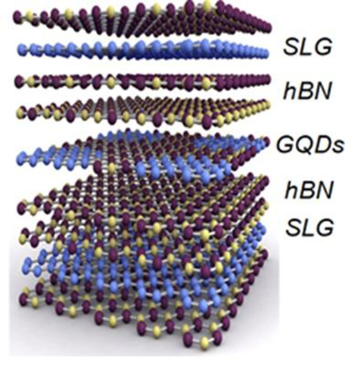
The schematic structure of the devices. Image: Davit Ghazaryan

Scientists from the Higher School of Economics, Manchester University, the Ulsan National Institute of Science & Technology and the Korea Institute of Science and Technology have developed a novel technology, which combines the fabrication procedures of planar and vertical heterostructures in order to assemble graphene-based single-electron transistors of excellent quality.

This technology could considerably expand the scope of research on two-dimensional materials by introducing a broader platform for the investigation of various devices and physical phenomena.

The manuscript is published as an article in Nature Communications.

In the study, it was demonstrated that high-quality graphene quantum dots (GQDs), regardless of whether they were ordered or randomly distributed, could be successfully synthesized in a matrix of monolayer hexagonal boron nitride (hBN).

Here, the growth of GQDs within the layer of hBN was shown to be catalytically supported by the platinum (Pt) nanoparticles distributed in-between the hBN and supporting oxidized silicon (SiO2) wafer, when the whole structure was treated by the heat in the methane gas (CH4). It was also shown, that due to the same lattice structure (hexagonal) and small lattice mismatch (~1.5 percent) of graphene and hBN, graphene islands grow in the hBN with passivated edge states, thereby giving rise to the formation of defectless quantum dots embedded in the hBN monolayer.

Such planar heterostructures incorporated by means of standard dry-transfer as mid-layers into the regular structure of vertical tunneling transistors (Si/SiO2/hBN/Gr/hBN/GQDs/hBN/Gr/hBN; here Gr refers to monolayer graphene and GQDs refers to the layer of hBN with the embedded graphene quantum dots) were studied through tunnel spectroscopy at low temperatures (3He, 250mK). The study demonstrated where the manifestation of well-established phenomena of the Coulomb blockade for each graphene quantum dot as a separate single electron transmission channel occurs.

“Although the outstanding quality of our single electron transistors could be used for the development of future electronics,” explains study co-author Davit Ghazaryan, Associate Professor at the HSE Faculty of Physics, and Research Fellow at the Institute of Solid State Physics (RAS). “This work is most valuable from a technological standpoint as it suggests a new platform for the investigation of physical properties of various materials through a combination of planar and van der Waals heterostructures.”

Related Articles Read More >

The emerging materials shaping next-generation semiconductor electronics
24 R&D trends that redefined 2024
Graphene-based flowmeter sensor measures nano-rate fluid flows, Part 3: The sensor
Graphene-based flowmeter sensor measures nano-rate fluid flows, Part 2: The graphene context
rd newsletter
EXPAND YOUR KNOWLEDGE AND STAY CONNECTED
Get the latest info on technologies, trends, and strategies in Research & Development.
RD 25 Power Index

R&D World Digital Issues

Fall 2024 issue

Browse the most current issue of R&D World and back issues in an easy to use high quality format. Clip, share and download with the leading R&D magazine today.

Research & Development World
  • Subscribe to R&D World Magazine
  • Enews Sign Up
  • Contact Us
  • About Us
  • Drug Discovery & Development
  • Pharmaceutical Processing
  • Global Funding Forecast

Copyright © 2025 WTWH Media LLC. All Rights Reserved. The material on this site may not be reproduced, distributed, transmitted, cached or otherwise used, except with the prior written permission of WTWH Media
Privacy Policy | Advertising | About Us

Search R&D World

  • R&D World Home
  • Topics
    • Aerospace
    • Automotive
    • Biotech
    • Careers
    • Chemistry
    • Environment
    • Energy
    • Life Science
    • Material Science
    • R&D Management
    • Physics
  • Technology
    • 3D Printing
    • A.I./Robotics
    • Software
    • Battery Technology
    • Controlled Environments
      • Cleanrooms
      • Graphene
      • Lasers
      • Regulations/Standards
      • Sensors
    • Imaging
    • Nanotechnology
    • Scientific Computing
      • Big Data
      • HPC/Supercomputing
      • Informatics
      • Security
    • Semiconductors
  • R&D Market Pulse
  • R&D 100
    • Call for Nominations: The 2025 R&D 100 Awards
    • R&D 100 Awards Event
    • R&D 100 Submissions
    • Winner Archive
    • Explore the 2024 R&D 100 award winners and finalists
  • Resources
    • Research Reports
    • Digital Issues
    • R&D Index
    • Subscribe
    • Video
    • Webinars
  • Global Funding Forecast
  • Top Labs
  • Advertise
  • SUBSCRIBE