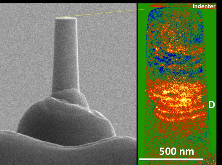
This is a dislocation avalanche in a high entropy nanopillar. Focused ion beam is used to fabricated the nanopillar (left) for compression test. Transmission electron microscope is used to image dislocation pile up during a dislocation avalanche (see D on the right). Credit: Frederick Seitz Materials Research Lab
Mechanical structures are only as sound as the materials from which they are made. For decades researchers have studied materials from these structures to see why and how they fail. Before catastrophic failure, there are individual cracks or dislocations that form, which are signals that a structure may be weakening. While researchers have studied individual dislocations in the past, a team from the University of Illinois at Urbana-Champaign, the University of Tennessee, and Oak Ridge National Laboratory has made it possible to understand how dislocations organize and react at nanoscale.
“Metals are made of polycrystals and the crystals have atoms arranged in an orderly way,” explained lead author Jian-Mu Zuo, Ivan Racheff Professor of Materials Science and Engineering and an affiliate with the Frederick Seitz Materials Research Lab at Illinois. “As force is applied in these metals, the crystal will slip and move against each other. A structure like a bridge might have a lot of dislocations, which can move, but the amount of movement is so small, it doesn’t have a consequence. However, as thousands or tens of thousands of dislocations tangle within a metal, and they produce local stress. This organization can lead to sudden deformation, like a snow avalanche. That’s very dramatic and much more difficult to control.”
The team, which also includes Illinois condensed matter physicist Karin Dahmen, published its results in Communications Physics. The experimental work was done by Dr. Yang Hu, as part of his Ph. D thesis.
Until this study researchers couldn’t make sense of the mechanism behind dislocation avalanche within a structure. However, the Illinois team found that a series of dislocations piling up forming a dam to prohibit movement. Behind the dam are tangled dislocations. Once there is enough pressure, an avalanche forms causing the dam to give way and sudden movement of the tangled dislocations, which weakens the metal and can eventually lead to catastrophic failure. By having a better understanding of this process, this study promises to aid in developing even stronger materials in the future and to better predict when a structure may be in peril.
In order to study the dislocations, which look like strings of as small as 10-9 meter in width, they followed the development of the dislocation avalanches in the compressed nanopillars of a high entropy alloy (HEA). The HEA has the same average structure as copper or gold. But the atoms are arranged in such a way to allow the researchers to do simultaneous measurements and to correlate dislocation motion with mechanical response and pinpoint exactly where the avalanche occurs. By identifying the dislocation bands, researchers are able to watch what happens before, during, and after the avalanche.
“People have understood how individual dislocations move, but until this point they haven’t understood how they move suddenly together,” Zuo noted. “Our innovation is to use a new material (the HEA) to study a very old problem and to develop this technique to do so.”
Because the dislocations typically structure themselves at microns apart (think the network of cracks in a sheet of ice after walking on it), it makes it hard to pinpoint a single event by looking at them inside a microscope that only works with thin samples (inside a transmission electron microscope, the sample thickness is typically less than a micron).
“In a conventional metal, the dislocations are too far apart than what we can see at one time, therefore they disappear on the surface” Zuo explained. “Also, a deformed metal has bunches of dislocations, but only a few that are actually active. Because of that, some scholars have commented when people look at the deformation afterward in the metal, it’s like visiting a dislocation graveyard.”
In order to witness a complete single avalanche, Zuo and his team needed to find a material where the dislocation interacts in a much smaller scale. The HEA is a new type of alloy comprised of five different metal elements (Al0.1CoCrFeNi). Because each metal atom has a different size and the crystal is distorted, it slows down the dislocation making it possible to store many dislocations and an avalanche within a relatively small volume.
The Illinois researchers were able measure the dislocation through a technique called nanoindentation. They take a piece of HEA and use an ion beam to fabricate a nanopillar and apply the force to the nanopillar with a small flat diamond tip of a nanoindenter.
“This material allows us to look at dislocations on the nanoscale (500 nanometers),” said Zuo, explaining the process. “We have a mechanical lab apply a force to a testing sample inside an electron microscope. As the stress is applied, the sample deforms. When stress exceeds the stress required for the dislocation to move inside the nanopillar, the dislocation will multiply. As the dislocation moves and encounters a resistance, they slow down and get tangled together and form a dislocation band. If you think of the stress like water flow, then the dislocation avalanche is like a dam breaking and water suddenly running out. The HEA makes the observation possible. “
The results of the process are two measurements – first a mechanical measurement, which allows the researchers to study how much force it takes for the dislocations to move and by how much, and secondly, electron imaging to capture the dislocation motion in a video. No study previously has been able to couple electron imaging and mechanical force measurement together to study dislocation avalanches.
“From previous accumulative studies, we knew how dislocations are produced and we have been able to study what was left behind,” Zuo said. “This study provides a critical answer to how dislocations interact.”
Zuo adds that this type of measurement can be used to develop theory and computational models that be used to predict how materials will behave under certain stress.
“That’s important because catastrophic failure starts with this type of sudden deformation,” Zuo said. “We will be able to better predict the action before there is catastrophic failure. That in turn should lead to the development of much stronger materials.”
This study coincides with strong efforts across the Illinois campus to use HEA for nuclear reactor and high temperature applications.
“HEAs are stable at high temperatures and can accommodate lots of strain,” Zuo said. “If we understand the dislocation structure, it will help to develop materials for very challenging applications.”


