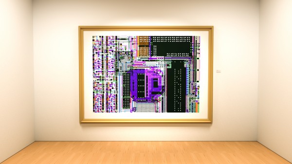
This illustration shows the layout of an application-specific integrated circuit, or ASIC, at an imaginary art exhibition. Members of the Integrated Circuits Department of SLAC’s Technology Innovation Directorate artfully design ASICs for a wide range of scientific experiments.
When Angelo Dragone talks about designing microchips for cutting-edge scientific applications at the Department of Energy’s SLAC National Accelerator Laboratory, it becomes immediately clear that it’s at least as much of an art form as it is research and engineering. Similar to the way painters follow an inspiration, carefully choose colors and place brush stroke after brush stroke on canvas, he says, electrical designers use their creative minds to develop the layout of a chip, draw electrical components and connect them to build complex circuitry.
Dragone leads a team of 12 design engineers who develop application-specific integrated circuits, or ASICs, for X-ray science, particle physics and other research areas at SLAC. Their custom chips are tailored to extract meaningful features from signals collected in the lab’s experiments and turn them into digital signals that can be further analyzed.
Like the CPU in your computer at home, ASICs process information and are extremely complex, with a 100 million transistors combined on a single chip, Dragone says. “However, while commercial integrated circuits are designed to be good at many things for broad use in all kinds of applications, ASICs are optimized to excel in a specific application.”
For SLAC applications this means, for example, that they perform well under harsh conditions, such as extreme temperatures at the South Pole and in space, as well as high levels of radiation in particle physics experiments. In addition, ultra-low-noise ASICs are designed to process signals that are extremely faint.
Pietro Caragiulo, a senior member of Dragone’s team, says, “Every chip we make is specific to the particular environment in which it’s used. That makes our jobs very challenging and exciting at the same time.”
From fundamental physics to self-driving cars
Most of the team’s ASICs are for SLAC’s core research areas in photon science and particle physics. First and foremost, ASICs are the heart of the ePix series of high-performance X-ray cameras that take snapshots of materials’ atomic fabric with the Linac Coherent Light Source (LCLS) X-ray laser.
“In a way, these ASICs play the same role in processing image information as the chip in your cell phone camera, but they operate under conditions that are way beyond the specifications of off-the-shelf technology,” Caragiulo says. They are, for instance, sensitive enough to detect single X-ray photons, which is crucial when analyzing very weak signals. They also have extremely high spatial resolution and are extremely fast, allowing researchers to make movies of atomic processes and study chemistry, biology and materials science like never before.
The engineers are now working on a new camera version for the LCLS-II upgrade of the X-ray laser, which will boost the machine’s frame rate from 120 to a million images per second and will pave the way for unprecedented studies that aim to develop transformative technologies, such as next-generation electronics, drugs and energy solutions. “X-ray cameras are the eyes of the machine, and all their functionality is implemented in ASICs,” Caragiulo says. “However, there is no camera in the world right now that is able to handle information at LCLS-II rates.”
In addition to X-ray applications at LCLS and the lab’s Stanford Synchrotron Radiation Lightsource (SSRL), ASICs are key components of particle physics experiments, such as the next-generation neutrino experiments nEXO and DUNE. The team is working on chips that will handle the data readout.
“The particular challenge here is that these experiments operate at very low temperatures,” says Bojan Markovic, another senior member of Dragone’s team. nEXO will run at minus 170 degrees Fahrenheit and DUNE at an even chillier minus 300 degrees, which is far below the temperature specifications of commercial chips.
Other challenges in particle physics include exposure to high particle radiation, for instance in the ATLAS detector at the Large Hadron Collider (LHC) at CERN in Europe. “In the case of ATLAS we also want ASICs that support a large number of pixels to obtain the highest possible spatial resolution, which is needed to determine where exactly a particle interaction occurred in the detector,” Markovic says.
SLAC’s ASICs can also be found in space. The Large Area Telescope on NASA’s Fermi Gamma-ray Space Telescope – a sensitive “eye” for the most energetic light in the universe – has 16,000 chips in nine different designs on board where they have been performing flawlessly for the past 10 years.
“We’re also expanding into areas that are beyond the research SLAC has traditionally been doing,” says Dragone whose Integrated Circuits Department is part of the Advanced Instrumentation for Research Division within the Technology Innovation Directorate that uses the lab’s core capabilities to foster technological advances. The design engineers are working with young companies to test their chips in a wide range of applications, including 3D sensing, the detection of explosives and driverless cars.
A creative process
But how exactly does the team develop a highly complex microchip and create its particular properties?
It all starts with a discussion in which scientists explain their needs for a particular experiment. “Our job as creative designers is to come up with novel architectures that provide the best solutions,” Dragone says.
After the requirements have been defined, the designers break the task down into smaller blocks. In the typical experimental scenario, a sensor detects a signal (like a particle passing through the detector) from which the ASIC extracts certain features (like the deposited charge or the time of the event) and converts them into digital signals which are then acquired and transported by an electronics board into a computer for analysis. The extraction block in the middle differs most from project to project and requires frequent modifications.
Once the team has an idea for how they want to do these modifications, they use dedicated computer systems to design the electronic circuits blocks, carefully choosing components to balance size, power, speed, noise, cost, lifetime and other specifications. Circuit by circuit, they draw the entire chip – an intricate three-dimensional layout of millions of electronic components and connections between them – and keep validating the design through simulations along the way.
“The way we lay everything out is key to giving an ASIC certain properties,” Markovic says. “For example, the mechanical or electrical shielding we put around the ASIC components prepares the chip for high radiation levels.”
The layout is sent to a foundry that fabricates a small-scale prototype, which is then tested at SLAC. Depending on the outcome of the tests, the layout is either modified or used to produce the final ASIC. Last but not least, Dragone’s team works with other groups in SLAC’s Technology Innovation Directorate that mate the ASICs with sensors and electronics boards.
“The time it takes from the initial discussion to having a functional chip varies with the complexity of the ASIC and depends on whether we’re modifying an existing design or building a completely new one,” Caragiulo says. “The entire process can take a couple of years, with three or four designers working on it.”
For the next few years, the main driver of ASICs development at SLAC is LCLS-II, which demands X-ray cameras that can snap images at unprecedented rates. Neutrino experiments and particle physics applications at the LHC will remain another focus, in addition to a continuing effort to expand into new fields and to work with start-ups.
The future for ASICs is bright, Dragone says. “We’re seeing a general trend to more and more complex experiments, and we need to put more and more complexity into our integrated circuits,” he says. “ASICs really make these experiments possible, and future generations of experiments will always need them.”
SSRL and LCLS are DOE Office of Science user facilities.