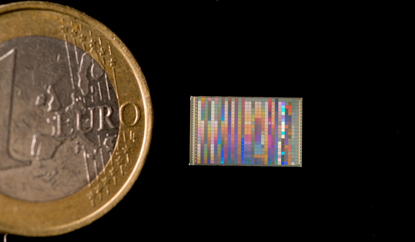
FOWINA – accurate micro color sensors for chip-level integration. Image: © K. Selsam, Fraunhofer ISC
In the FOWINA project, the Fraunhofer Institute for Integrated Circuits IIS in Erlangen and the Fraunhofer Institute for Silicate Research ISC in Würzburg have developed novel color sensors with a special microlens arrangement.
The sensors can be realized directly on the chip and combine multiple functions in a minimum of space. Their extremely slim design makes the sensors suitable for a wide range of applications, such as in mobile devices or color-adjustable LED lamps.
Color sensors are used in displays, LEDs and other tech devices to generate true colors. Their fabrication involves the use of special nanoplasmonic structures. These structures filter the incident light, allowing only precisely defined regions of the color spectrum to reach the detector surface. The ability to control the angle of incidence is decisive to the correct functioning of the color filters.
Conventional sensors contain macroscopic elements to improve the filter’s accuracy and avoid untrue colors by masking out light at undesirable angles, but these added elements significantly increase the component’s build size.
To overcome this drawback, the two Fraunhofer Institutes working on the FOWINA project, IIS and ISC, are developing an all-in-one solution that combines multiple functions in a minimum of space. Color-filter structures, angular filters to regulate the incident light, evaluation circuits for signal processing, and photodiodes to convert light energy into electrical energy are all integrated in the color sensor chip.
This extremely compact design makes it possible to build novel, ultraslim color sensors for incorporation in cameras, smartphones, and many other products.
FOWINA is an in-house project funded by Fraunhofer as part of its internal program of SME-oriented research. The German acronym stands for “controlling the angular spectrum of nanostructured color sensors using micro-optical beam-shaping elements.”
As well as their high scale of integration, which allows a maximum of functions to be packed onto a small surface, the novel sensors are easier and thus less expensive to fabricate than their predecessors. Fraunhofer IIS is responsible for developing the sensor IC including the nanoplasmonic color filters. The latter can be manufactured costefficiently together with the photodiodes and evaluation circuits using one and the same CMOS process, i.e. a single technology.
Fraunhofer ISC is responsible for fabricating the arrays of microstructures that serve as the angular filter elements in the sensors. “
We use the advanced technique of two-photon polymerization, which enables the creation of almost any type of microstructure or structured surface,” says Dr. Sönke Steenhusen, a research scientist at Fraunhofer ISC.
To speed up the manufacturing process, Fraunhofer ISC employs nanoimprint technology — a highly precise and field-proven lithographic technique — to replicate the microstructures. This method also allows different structures to be combined on the same substrate.
In the course of the FOWINA project, Fraunhofer ISC has achieved the best-possible color-filter performance by restricting the angle of incident light to a tolerance range of +/-10 degrees using micro-optical structures. This enables the color of LEDs, for example, to be actively adjusted.
Another plus point is the very high surface accuracy of the microlenses, which focus the light on the color filters in a targeted manner. The material used by Fraunhofer ISC to fabricate the arrays is a special inorganic-organic hybrid polymer, which exhibits high chemical, thermal and mechanical stability and can be easily adapted to the requirements of specific applications by modifying its molecular structure.
The two collaborating Fraunhofer Institutes are currently optimizing the design and manufacturing processes for the color sensors, with a view to scaling up to industrial applications and, at a later date, mass production of the sensors.
Source: Fraunhofer Institute


