Image of the Greek goddess Minerva as seen under a fused silica substrate with 450 nm nanopillars on both sides (left) compared to an unstructured reference (right). Each substrate has a diameter of 25 mm, matching the size of the drawing. The top set of images were taken at an observation angle of 0 degrees, the bottom set of images at an observation angle of 30 degrees. Image: © Zhaolu Diao
Most lenses, objectives, eyeglass lenses, and lasers come with an anti-reflective coating. Unfortunately, this coating works optimally only within a narrow wavelength range. Scientists at the Max Planck Institute for Intelligent Systems in Stuttgart have now introduced an alternative technology. Instead of coating a surface, they manipulate the surface itself. By comparison with conventional procedures, this provides the desired anti-reflective effect across a wider wavelength range. But more than this, it largely increases the light transmittance through surfaces. In the future, the nanostructured surfaces may improve high-energy lasers as well as touchscreens and the output of solar modules.
Researchers at the Max Planck Institute for Intelligent Systems took a page out of the design book for moth cornea. The corneas of these mostly nocturnal insects reflect almost no incoming light. There is no glow of light bouncing off the moth’s eyes to betray their presence to potential predators. Less reflected light also means that moths are able to use practically all the scarce night-time light to see.
This magic from the world of insects inspired scientists to try the same tactics for the design of optical components. Like the corneas of moths, the components must allow light to pass through while light reflection is of little use. So far, component designers apply anti-reflective coating to lenses, display screens, monitors, and laser components. However, these coatings have disadvantages. Most of them work only in a narrow wavelength range, and they produce lens errors dependent on the angle of light incidence.
Applying the moth cornea principle will put an end to these problems. Scientists at the Max Planck Institute for Intelligent Systems, Department for New Materials and Biosystems, under the guidance of Director Joachim Spatz had a good look at their natural model. Physicist Zhaolu Diao explains nature’s design: “The eye surface is densely covered with column-like structures. They are only a few hundred nanometres high and taper conically toward the tip.” The columns look like regularly spaced stalagmites on a cavern floor. As the light passes through this boundary layer, its refractive index changes continuously, starting from the ambient air to the materials of the outer moth eye layers.
This gradual refractive index change has the effect that the layer hardly reflects any of the incoming light. Instead, almost all incoming light penetrates into the eye. By contrast, when incoming light hits a smooth surface, the refractive index will change abruptly. Based on the laws of physics, this will cause light reflection. Diao adds another important prerequisite: “To make the system work, the distances between individual columns must be significantly smaller than the wavelength of the incoming light.”
To imitate the moth eye principle, the scientists needed to find a way of turning smooth surfaces into nano-column landscapes. To accomplish this, they developed a two-step process. In the first step, they deposited gold particles in a regular honeycomb pattern on a large surface. In this regular honeycomb pattern, the gold particles settle in the points of crossroad. In the second step, the gold-studded crossroads serve as mask in a chemical etching process. As a result, no material is etched away underneath the gold-studded crossroads, and the desired upright column-like structures remain. The structured surfaces covered as much as two by two centimeters.
While this technique registered first successes in the past, it has so far only worked for short wave UV radiation and visible light. However, the same was not the case for the longer wavelengths of near infrared light (NIR). The reason for this was the column size. Until then, the columns etched out of the surface were at most 500 nanometers high. The columns are not high enough to reach the 99.5 percent or higher light transmittance for the wavelengths in the NIR range. “The longer the light waves, the higher we must build the nanostructures,” explains Diao.
The group fine-tuned their procedures and found a way to increase the size of the deposited gold particles. “This made it possible for us to etch deeper into the material,” reports Diao. The scientists were now able to etch out columns as high as 2,000 nanometers or two micrometers, four times as high as before.
The new techniques also allow the scientists to influence the shape of the nano-columns. They control the way in which the columns taper from the bottom to the top and how narrow they are on the top. In the process, they learned that evenly tapered columns will permit the highest transmittance rates.
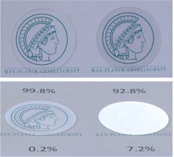
The scientists experimented with various column heights and confirmed that they achieved the best transmittance values for different wavelengths with different heights they made the columns. For 1.95 micrometer-high columns, the transmittance maximum was 99.8 percent, clearly in the NIR at almost 2.4 micrometers. With increasing column height, the range of wavelengths with high transmittance widened. For 1.95 micrometer high column layers, the high transmittance rates of 99.5 percent or higher covered about 450 nanometers of the spectrum. For smaller column structures, the high-transmittance window was only 250 nanometers wide.
High transmittance rates together with much reduced light reflection are the basis for possible ‘stealth applications’ because the surface-treated materials are optically indistinguishable from their environment. After column etching a piece of quartz glass, people did not see the outlines of the piece of quartz glass in front of them, and a camera did not record them. But when the Max Planck scientists covered an image with a piece of quartz glass with column-studded surface, the image remained clearly visible even if viewed at an acute angle and from the upper edge (see illustration). In contrast, quartz glass with unmodified surface reflected the incoming light so much that onlookers no longer recognized anything at an angle of only 30 degrees.
In the first experimental phase, the scientists tested their hypotheses using quartz glass. Future plans include testing the techniques on optical lenses and sapphires. As soon as the techniques have proven applicable to the new materials, the scientist will be eager to test the many possible applications. Many applications could certainly benefit from the use of components with next to no reflection across a wide range of wavelengths and up to 99.8 percent transmittance of incoming light. “One important field would be high-energy lasers operating in the infra-red range,” asserts Diao. Especially in certain laser systems, in which the light is amplified while it passes through the same optical components again and again, small losses through reflection will add up to noticeable energy losses. “Twenty-three percent of the energy will be lost after the same light beam hits the same boundary fifty times at a transmittance of 99.5 percent,” points out Diao. At 99.8 percent transmittance, the total energy loss after 50 passages would be only 10 percent. Furthermore, in field tests, the nanostructured surfaces are far more resilient against the high laser energy than anti-reflective coatings. This is another advantage especially for laser applications.
Other feasible applications could be lenses, objectives, or touchscreens. Nanostructured surfaces offer yet another advantage. Diao points out: “The technique is not only suitable for level, but also for curved surfaces. That would be beneficial especially for camera or microscope lenses. Before the technique can help improve touchscreens, a solution must be found for the problem of contamination via touch. Experiments have shown that touch by human hands will leave obvious traces. Over time, this will seriously impair the surface and lead to significantly reduced transmittance. On the bright side, the scientists were also able to show how easily touchscreen users can wipe away such contamination with a little laboratory alcohol as easy as from a glass surface. Still for touchscreen applications, the scientists still expect to find a more elegant solution.
Source: Max Planck Institute