Research & Development World

  • R&D World Home
  • Topics
    • Aerospace
    • Automotive
    • Biotech
    • Careers
    • Chemistry
    • Environment
    • Energy
    • Life Science
    • Material Science
    • R&D Management
    • Physics
  • Technology
    • 3D Printing
    • A.I./Robotics
    • Software
    • Battery Technology
    • Controlled Environments
      • Cleanrooms
      • Graphene
      • Lasers
      • Regulations/Standards
      • Sensors
    • Imaging
    • Nanotechnology
    • Scientific Computing
      • Big Data
      • HPC/Supercomputing
      • Informatics
      • Security
    • Semiconductors
  • R&D Market Pulse
  • R&D 100
    • Call for Nominations: The 2025 R&D 100 Awards
    • R&D 100 Awards Event
    • R&D 100 Submissions
    • Winner Archive
    • Explore the 2024 R&D 100 award winners and finalists
  • Resources
    • Research Reports
    • Digital Issues
    • R&D Index
    • Subscribe
    • Video
    • Webinars
  • Global Funding Forecast
  • Top Labs
  • Advertise
  • SUBSCRIBE

Levitating 2D Semiconductor Offers Superior Performance

By KAIST | August 28, 2018

Atomically thin 2D semiconductors have been drawing attention for their superior physical properties over silicon semiconductors; nevertheless, they are not the most appealing materials due to their structural instability and costly manufacturing process. To shed some light on these limitations, a KAIST research team suspended a 2D semiconductor on a dome-shaped nanostructure to produce a highly efficient semiconductor at a low cost.

2D semiconducting materials have emerged as alternatives for silicon-based semiconductors because of their inherent flexibility, high transparency, and excellent carrier transport properties, which are the important characteristics for flexible electronics.

Despite their outstanding physical and chemical properties, they are oversensitive to their environment due to their extremely thin nature. Hence, any irregularities in the supporting surface can affect the properties of 2D semiconductors and make it more difficult to produce reliable and well performing devices. In particular, it can result in serious degradation of charge-carrier mobility or light-emission yield.

To solve this problem, there have been continued efforts to fundamentally block the substrate effects. One way is to suspend a 2D semiconductor; however, this method will degrade mechanical durability due to the absence of a supporter underneath the 2D semiconducting materials.

Professor Yeon Sik Jung from the Department of Materials Science and Engineering and his team came up with a new strategy based on the insertion of high-density topographic patterns as a nanogap-containing supporter between 2D materials and the substrate in order to mitigate their contact and to block the substrate-induced unwanted effects.

More than 90 percent of the dome-shaped supporter is simply an empty space because of its nanometer scale size. Placing a 2D semiconductor on this structure creates a similar effect to levitating the layer. Hence, this method secures the mechanical durability of the device while minimizing the undesired effects from the substrate. By applying this method to the 2D semiconductor, the charge-carrier mobility was more than doubled, showing a significant improvement of the performance of the 2D semiconductor.

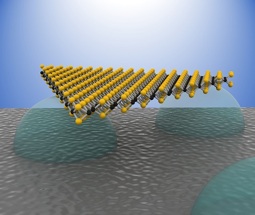
Image of a 2D semiconductor using dome structures.

Additionally, the team reduced the price of manufacturing the semiconductor. In general, constructing an ultra-fine dome structure on a surface generally involves costly equipment to create individual patterns on the surface. However, the team employed a method of self-assembling nanopatterns in which molecules assemble themselves to form a nanostructure. This method led to reducing production costs and showed good compatibility with conventional semiconductor manufacturing processes.

Jung says, “This research can be applied to improve devices using various 2D semiconducting materials as well as devices using graphene, a metallic 2D material. It will be useful in a broad range of applications, such as the material for the high speed transistor channels for next-generation flexible displays or for the active layer in light detectors.”

This research, led by PhD candidate Soomin Yim, was published in Nano Letters in April.

Source: KAIST

Related Articles Read More >

TSMC’s N3P hits mass production, with N3X customer sampling slated for Q3–Q4 2025a
7 major R&D developments this week: Tariff uncertainty persists, Pfizer sells campus, Scania acquires Northvolt unit
While Trump tariffs spare phones/PCs, R&D could faces GPU cost pressures
Why IBM predicts quantum advantage within two years
rd newsletter
EXPAND YOUR KNOWLEDGE AND STAY CONNECTED
Get the latest info on technologies, trends, and strategies in Research & Development.
RD 25 Power Index

R&D World Digital Issues

Fall 2024 issue

Browse the most current issue of R&D World and back issues in an easy to use high quality format. Clip, share and download with the leading R&D magazine today.

Research & Development World
  • Subscribe to R&D World Magazine
  • Enews Sign Up
  • Contact Us
  • About Us
  • Drug Discovery & Development
  • Pharmaceutical Processing
  • Global Funding Forecast

Copyright © 2025 WTWH Media LLC. All Rights Reserved. The material on this site may not be reproduced, distributed, transmitted, cached or otherwise used, except with the prior written permission of WTWH Media
Privacy Policy | Advertising | About Us

Search R&D World

  • R&D World Home
  • Topics
    • Aerospace
    • Automotive
    • Biotech
    • Careers
    • Chemistry
    • Environment
    • Energy
    • Life Science
    • Material Science
    • R&D Management
    • Physics
  • Technology
    • 3D Printing
    • A.I./Robotics
    • Software
    • Battery Technology
    • Controlled Environments
      • Cleanrooms
      • Graphene
      • Lasers
      • Regulations/Standards
      • Sensors
    • Imaging
    • Nanotechnology
    • Scientific Computing
      • Big Data
      • HPC/Supercomputing
      • Informatics
      • Security
    • Semiconductors
  • R&D Market Pulse
  • R&D 100
    • Call for Nominations: The 2025 R&D 100 Awards
    • R&D 100 Awards Event
    • R&D 100 Submissions
    • Winner Archive
    • Explore the 2024 R&D 100 award winners and finalists
  • Resources
    • Research Reports
    • Digital Issues
    • R&D Index
    • Subscribe
    • Video
    • Webinars
  • Global Funding Forecast
  • Top Labs
  • Advertise
  • SUBSCRIBE