Research & Development World

  • Home Page
  • Topics
    • Aerospace
    • Archeology
    • Automotive
    • Biotech
    • Chemistry
    • Environment
    • Energy
    • Life Science
    • Material Science
    • R&D Market Pulse
    • R&D Management
    • Physics
  • Technology
    • 3D Printing
    • A.I./Robotics
    • Battery Technology
    • Imaging
    • Nanotechnology
    • Semiconductors
  • Controlled Environments
    • Cleanrooms
    • Graphene
    • Lasers
    • Regulations/Standards
    • Sensors
  • Scientific Computing
    • Big Data
    • HPC/Supercomputing
    • Informatics
    • Security
    • Software
  • R&D 100 Awards
    • ENTER NOW
    • 2020 Winners
    • Winner Archive
    • R&D 100 Conference
  • Resources
    • Digital Issues
    • Podcasts
    • Subscribe
  • 2021 Funding Forecast
  • COVID-19

Mass Production of New Class of Semiconductors Closer to Reality

By University of Waterloo | February 9, 2018

Two Waterloo chemists have made it easier for manufacturers to produce a new class of faster and cheaper semiconductors.

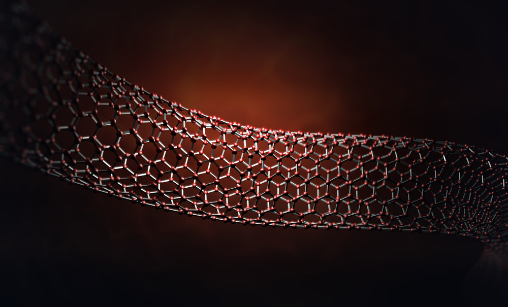
The chemists have found a way to simultaneously control the orientation and select the size of single-walled carbon nanotubes deposited on a surface. That means the developers of semiconductors can use carbon as opposed to silicon, which will reduce the size and increase the speed of the devices while improving their battery life.

“We’re reaching the limits of what’s physically possible with silicon-based devices,” said co-author Derek Schipper, Canada Research Chair Organic Material Synthesis at the University of Waterloo. “Not only would single-walled carbon nanotube-based electronics be more powerful, they would also consume less power.”

The process, called the Alignment Relay Technique, relies on liquid crystals to pass orientation information to a metal-oxide surface. Small molecules called iptycenes then bond to the surface locking the orientation pattern into place. Their structure includes a small pocket large enough to fit a certain size carbon nanotube that remains after washing.

“This is the first time chemists have been able to externally control the orientation of small molecules covalently bonded to a surface,” said Schipper, a professor of chemistry and a member of the Waterloo Institute for Nanotechnology. “We’re not the first ones to come up with potential solutions to work with carbon nanotubes. But this is the only one that tackles both orientation and purity challenges at the same time.”

Schipper further pointed out that the approach is from the bottom up with the use of organic chemistry to design and build a molecule which then does the hard work.

“Once you’ve built the pieces, the process is simple. It’s a bench-top method requiring no special equipment,” Schipper explained.

In contrast to self-assembly techniques which rely on the design of a suitable molecule to fit snuggly together, this process can be controlled at every step, including the size of the iptycene “pocket”. In addition, this is the first a solution has been found to tackling the challenge of aligning and purifying carbon nanotubes at the same time.

Related Articles Read More >

With this new science, plastics could see a second life as biodegradable surfactants
Tires turned into graphene that makes stronger concrete
Wafer-thin nanopaper changes from firm to soft at the touch of a button
Airplanes to cellphones: New equipment finds the flaws in everything

Need R&D World news in a minute?

We Deliver!
R&D World Enewsletters get you caught up on all the mission critical news you need in research and development. Sign up today.
Enews Signup
Tweets by @RandDWorld

R&D World Digital Issues

February 2020 issue

Browse the most current issue of R&D World and back issues in an easy to use high quality format. Clip, share and download with the leading R& magazine today.

Research & Development World
  • Subscribe to R&D World Magazine
  • Enews Sign Up
  • Contact Us
  • Drug Discovery & Development
  • Pharmaceutical Processing
  • 2021 Global Funding Forecast

Copyright © 2021 WTWH Media LLC. All Rights Reserved. The material on this site may not be reproduced, distributed, transmitted, cached or otherwise used, except with the prior written permission of WTWH Media
Privacy Policy | Advertising | About Us

Search R&D World

  • Home Page
  • Topics
    • Aerospace
    • Archeology
    • Automotive
    • Biotech
    • Chemistry
    • Environment
    • Energy
    • Life Science
    • Material Science
    • R&D Market Pulse
    • R&D Management
    • Physics
  • Technology
    • 3D Printing
    • A.I./Robotics
    • Battery Technology
    • Imaging
    • Nanotechnology
    • Semiconductors
  • Controlled Environments
    • Cleanrooms
    • Graphene
    • Lasers
    • Regulations/Standards
    • Sensors
  • Scientific Computing
    • Big Data
    • HPC/Supercomputing
    • Informatics
    • Security
    • Software
  • R&D 100 Awards
    • ENTER NOW
    • 2020 Winners
    • Winner Archive
    • R&D 100 Conference
  • Resources
    • Digital Issues
    • Podcasts
    • Subscribe
  • 2021 Funding Forecast
  • COVID-19