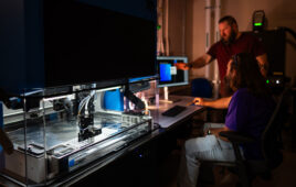
The experimental setup in Professor Eric Mazur’s laser laboratory at Harvard University. Using femtosecond lasers, Mazur and colleagues have developed a new nanofabrication process for use in creating metamaterials. Image: Harvard University |

Researchers in applied physics have
cleared an important hurdle in the development of advanced materials, called
metamaterials, that bend light in unusual ways.
Working at a scale applicable to infrared
light, the Harvard
University team has used
extremely short and powerful laser pulses to create 3D patterns of tiny silver
dots within a material. Those suspended metal dots are essential for building
futuristic devices like invisibility cloaks.
The new fabrication process, described in Applied Physics Letters,
advances nanoscale metal lithography into three dimensions—and does it at a
resolution high enough to be practical for metamaterials.
“If you want a bulk metamaterial for
visible and infrared light, you need to embed particles of silver or gold
inside a dielectric, and you need to do it in 3D, with high resolution,”
says lead author Kevin Vora, a graduate student at the Harvard School of
Engineering and Applied Sciences (SEAS).
“This work demonstrates that we can
create silver dots that are disconnected in x,
y, and z,” Vora says.
“There’s no other technique that feasibly allows you to do that. Being
able to make patterns of nanostructures in 3D is a very big step towards the
goal of making bulk metamaterials.”
Vora works in the laboratory of Eric
Mazur, Balkanski Professor of Physics and Applied Physics at SEAS. For decades,
Mazur has been using a piece of equipment called a femtosecond laser to
investigate how very tightly focused, powerful bursts of light can change the
electrical, optical, and physical properties of a material.
When a conventional laser shines on a
transparent material, the light passes straight through, with slight
refraction. The femtosecond laser is special because it emits a burst of
photons as bright as the surface of the sun in a flash lasting only 50
quadrillionths of a second. Instead of shining through the material, that
energy gets trapped within it, exciting the electrons within the material and
achieving a phenomenon known as nonlinear absorption.
|

Inside the pocket where that energy is
trapped, a chemical reaction can take place, permanently altering the internal
structure of the material. The process has previously been exploited for 2D and
simple 3D metal nanofabrication.
“Normally, when people use
femtosecond lasers in fabrication, they’re creating a wood pile structure:
something stacked on something else, being supported by something else,”
explains Mazur.
“If you want to make an array of
silver dots, however, they can’t float in space.”
In the new process, Vora, Mazur, and their
colleagues combine silver nitrate, water, and a polymer called PVP into a
solution, which they bake onto a glass slide. The solid polymer then contains
ions of silver, which are photoreduced by the tightly focused laser pulses to
form nanocrystals of silver metal, supported by the polymer matrix.
The need for this particular combination
of chemicals, at the right concentrations, was not obvious in prior work.
Researchers sometimes combine silver nitrate with water in order to create
silver nanostructures, but that process provides no structural support for a 3D
pattern. Another process combines silver nitrate, water, PVP, and ethanol, but
the samples darken and degrade very quickly by producing silver crystals throughout
the polymer.
With ethanol, the reaction happens too
quickly and uncontrollably. Mazur’s team needed nanoscale crystals, precisely
distributed and isolated in 3D.
“It was just a question of removing
that reagent, and we got lucky,” Vora says. “What was most surprising
about it was how simple it is. It was a matter of using less.”