Research & Development World

  • R&D World Home
  • Topics
    • Aerospace
    • Automotive
    • Biotech
    • Careers
    • Chemistry
    • Environment
    • Energy
    • Life Science
    • Material Science
    • R&D Management
    • Physics
  • Technology
    • 3D Printing
    • A.I./Robotics
    • Software
    • Battery Technology
    • Controlled Environments
      • Cleanrooms
      • Graphene
      • Lasers
      • Regulations/Standards
      • Sensors
    • Imaging
    • Nanotechnology
    • Scientific Computing
      • Big Data
      • HPC/Supercomputing
      • Informatics
      • Security
    • Semiconductors
  • R&D Market Pulse
  • R&D 100
    • Call for Nominations: The 2025 R&D 100 Awards
    • R&D 100 Awards Event
    • R&D 100 Submissions
    • Winner Archive
    • Explore the 2024 R&D 100 award winners and finalists
  • Resources
    • Research Reports
    • Digital Issues
    • R&D Index
    • Subscribe
    • Video
    • Webinars
  • Global Funding Forecast
  • Top Labs
  • Advertise
  • SUBSCRIBE

Multitasking Monolayers Lay Groundwork for Dual-Function Devices

By Vanderbilt University | July 25, 2017

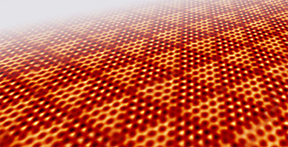
Illustration of the triangular pattern formed by the two-dimensional material chalcogenide that allows the creation of dual-function devices. (Yu-Yang Zhang / Chinese Academy of Sciences)

Two-dimensional materials that can multitask.

That is the result of a new process that naturally produces patterned monolayers that can act as a base for creating a wide variety of novel materials with dual optical, magnetic, catalytic or sensing capabilities.

“Patterned materials open up the possibility of having two functionalities in a single material, such as catalyzing a chemical reaction while simultaneously serving as a sensor for a second set of molecules,” said Sokrates Pantelides, William and Nancy McMinn Professor of Physics at Vanderbilt University, who coordinated the research with Professor Hong-Jun Gao at the Institute of Physics of the Chinese Academy of Sciences in Beijing. “Of course, you can do such a thing by using two materials side by side, but patterned materials offer a whole range of new options for device designers.”

Their achievement is described in a paper titled “Intrinsically patterned two-dimensional materials for selective adsorption of molecules and nanoclusters” published Jun. 12 in the journal Nature Materials.

In electronics, two dimensional (2D) materials are a hot topic because of their many potential applications. Graphene, which consists of a single sheet of carbon atoms, has received the most attention, but it has proven very difficult to tune its chemical and electrical properties. As a result, chalcogenides (materials that contain sulfur, selenium or tellurium, which are known for their widely varied optical, electrical and thermal properties) are now the focus of worldwide research because some of them naturally form monolayers that can serve as blank slates that are readily tailored for specific applications.

Now, Pantelides and his collaborators have shown that monolayers formed by two chalcogenides (platinum-selenium and copper-selenium) naturally combine with nanoscale precision into alternating triangles with different phases: metallic and semiconductor. Because each phase has different electrical and chemical properties, two different types of molecules can bond to its surface, allowing it to perform two functions simultaneously.

“In general, 2D materials are ‘functionalized’ for specific applications by adsorbing different species of atoms or molecules on them or by embedding impurities in their otherwise perfect crystalline structure in the same way that semiconductors such as silicon are functionalized by doping with impurities, which enables the fabrication of electronic devices, such as the ‘chips’ that drive computers,” Pantelides explained. “Our new paper extends the realm of 2D materials by one important step. It demonstrates a way to fabricate 2D materials that allows the two phases of the material to be functionalized independently.”

The experiments were conducted in Gao’s laboratory in Beijing and theoretical calculations were performed at Vanderbilt, the U.S Department of Energy’s National Energy Research Scientific Computing Center and the University of the Chinese Academy of Sciences.

Related Articles Read More >

KIST carbon nanotube supercapacitor holds capacity after 100,000 cycles
A new wave of metalworking lets semiconductor crystals bend and stretch
LLNL deposits quantum dots on corrugated IR chips in a single step
KATRIN inauguration photo form 2018
Neutrinos pinned below 0.45 eV; KATRIN halves the particle’s mass ceiling
rd newsletter
EXPAND YOUR KNOWLEDGE AND STAY CONNECTED
Get the latest info on technologies, trends, and strategies in Research & Development.
RD 25 Power Index

R&D World Digital Issues

Fall 2024 issue

Browse the most current issue of R&D World and back issues in an easy to use high quality format. Clip, share and download with the leading R&D magazine today.

Research & Development World
  • Subscribe to R&D World Magazine
  • Enews Sign Up
  • Contact Us
  • About Us
  • Drug Discovery & Development
  • Pharmaceutical Processing
  • Global Funding Forecast

Copyright © 2025 WTWH Media LLC. All Rights Reserved. The material on this site may not be reproduced, distributed, transmitted, cached or otherwise used, except with the prior written permission of WTWH Media
Privacy Policy | Advertising | About Us

Search R&D World

  • R&D World Home
  • Topics
    • Aerospace
    • Automotive
    • Biotech
    • Careers
    • Chemistry
    • Environment
    • Energy
    • Life Science
    • Material Science
    • R&D Management
    • Physics
  • Technology
    • 3D Printing
    • A.I./Robotics
    • Software
    • Battery Technology
    • Controlled Environments
      • Cleanrooms
      • Graphene
      • Lasers
      • Regulations/Standards
      • Sensors
    • Imaging
    • Nanotechnology
    • Scientific Computing
      • Big Data
      • HPC/Supercomputing
      • Informatics
      • Security
    • Semiconductors
  • R&D Market Pulse
  • R&D 100
    • Call for Nominations: The 2025 R&D 100 Awards
    • R&D 100 Awards Event
    • R&D 100 Submissions
    • Winner Archive
    • Explore the 2024 R&D 100 award winners and finalists
  • Resources
    • Research Reports
    • Digital Issues
    • R&D Index
    • Subscribe
    • Video
    • Webinars
  • Global Funding Forecast
  • Top Labs
  • Advertise
  • SUBSCRIBE