It would be nice to be able to build a typical laboratory and command that “thou shall conduct nanoscale research here.” However, as nanoscale research evolves so must the architecture and building technologies.
Nanotechnology is not the new emerging science that the mainstream media would have us believe. In fact, nanotechnology has been present on scientists’ radar for over two decades. Over the past decade, and particularly the past five years, there have been amazing strides in nanotechnology research and product development. Many of these accomplishments are due in large part to the facilities built to meet the stringent requirements presented by many nanometer scale research programs. Existing design and construction guidelines do not fully address the requirements of this new facility type. This article will address the state of emerging guidelines and recommended practices and discuss the array of technical and human criteria that emerge in the design of laboratories and cleanrooms supporting nanoscale science and technology laboratories. Subsequent articles in this series will focus on individual topics and building case studies.
LOOK FOR THE NEW IEST GUIDELINES
During the past few years, a number of nanotech facilities have been constructed and are now fully operational. During this time, the Institute of Environmental Sciences and Technology (IEST) has derived important practical information from these nanotech facilities.
I have been involved in the design of nanotech facilities for the past eighteen years, and I currently co-chair IEST’s Working Group NANO-200 dedicated to publishing the first set of guidelines that will address nanotech research and production facilities. These guidelines will be published within the next few months and will address planning, design, construction, and operational considerations for facilities engaged in research or production at the nanometer scale.
ESTABLISHING TECHNICAL REQUIREMENTS FOR A PROJECT
Establishing technical requirements is the important first-step to designing a building that will not become prematurely obsolete. Nanoscale research is a vast and complicated field of study that can engage a wide range of disciplines from both basic and applied science. Inherent in the nature of emerging areas of research, of program,and of a specific location are requirements that make each project unique: there is no standard design solution. In reality, many types of nanoscale research require specialized laboratories designed to meet an array of special criteria. It is not unusual for conflicts to arise in the technical criteria as spaces are integrated. For example, some spaces may need an environment clear of airborne particulates; others require severely limited vibration and noise; while temperature and humidity control must be maintained in other areas. The need for large air handling equipment used to control temperature and humidity in one area will affect the stringent vibration and noise limits required in other areas.
The complex mix of technical requirements for nanoscale research are aimed at creating an interior environment that is extremely controlled, to a degree far exceeding other research facilities, both for the science itself and for proper operation of equipment. It is important to note that there are nanotechnology applications that can and do occur in standard chemistry laboratories. However, conducting atomic level measurements and characterization, as well as nanofabrication and other functions typically found in nanoscale research often require critical environments that demand tighter control of the fluctuation of environmental characteristics within the laboratory. These technical considerations might involve controlling temperature and humidity levels, isolating vibration and acoustic noise, reducing the quantity and size of airborne particulates, and shielding from electrical, electromagnetic, and radio frequency interferences. Electron microscopes are most sensitive to many of the above “noise” sources. Additionally, temperature fluctuation along the length of a laser beam could cause distortion and therefore lose focus and accuracy in measurements. The beam could also be misaligned by vibrations while electromagnetic interference causes the wavelength to change introducing errors in measurements.
The specially designed facility at the National Physical Laboratory (NPL) in Teddington, UK provides a unique example where a variety of laboratories requiring various technical criteria heavily influenced the overall masterplan of the campus (Figure 1). The campus masterplan included a network of interconnected buildings designed as separate “modules.” Each building module was dedicated to a particular measurement science, which in turn required a high level of control over the various environmental criteria. This resulted in a group of buildings that look similar on the outside, but are specifically designed and engineered for a particular function.

TEMPERATURE AND HUMIDITY CONTROL
Achieving a certain temperature and keeping it constant can be more difficult than it seems. Work conducted in the lab can change the ambient temperature enough to interfere with the experiment. Temperature can be closely controlled and maintained by designing systems that circulate the volume of air inside the room with a high number of air changes per hour. In typical laboratories, temperature fluctuations are controlled to ± 1 degree Celsius. Closer temperature control is sometimes needed and the tolerance can range from 0.5 degree Celsius down to a range of ±0.01 degree Celsius in highly critical spaces. Similarly, humidity control, depending on the research requirements, may vary between ± 5% down to 1% of relative humidity (RH).
The National Institute of Standards and Technology (NIST) Advanced Measurement Laboratory project (AML) provides the best examples of how to deal with tightly controlled environments in a nanoscale research facility. The NIST AML baseline average room air temperature for all laboratories is controlled to within ±0.25 degree Celsius. There are 48 precision temperature control laboratories located in two underground metrology wings requiring temperature control to within ±0.1 or ±0.01 degree Celsius and humidity control to 1% of RH. Such laboratories were designed to house highly specialized experiments such as the Molecular Measuring Machine (M3), an instrument designed to draw lines on silicon as small as 10 nanometers wide and 4 nanometers high (Figure 2). It can also measure the placement of nanoscale features with subnanometer resolution. Arrays of high-precision thermistors and humidity sensors were used to control the temperature. These were individually calibrated by NIST researchers to ensure a tolerance of less than ±0.003 degree. This extreme accuracy is necessary for input into the precision direct-digital-control systems serving the AML laboratories, keeping the spaces controlled within the specified criteria.

VIBRATION ISOLATION
Vibration is an important and complex issue. When measuring or capturing an image at the atomic scale, the slightest vibration can invalidate results; even extremely small motions can distort images created by an electron microscope. First, the level of vibration that can be tolerated must be determined. It is equally important to test the potential site at the outset to gauge ambient vibration levels, both during the day and at night. Once the threshold is set and the site’s vibration level is identified, then building design options can be considered. The more stringent the requirement, the more expensive the structure will be. A solution could be as simple as setting the building back an adequate distance from the street to minimize the vibration caused by traffic. However, not all building sites can provide for such setbacks.
The Sandia National Laboratories Center for Integrated Nanotechnologies (CINT) in Albuquerque, NM (Figure 3) is an example where the building was located outside the perimeter of the main campus in order to provide more distance between the building and outside noise environment. This further isolated the building from potential noise generated from surrounding buildings and it provided greater distance between the facility and vehicular traffic. Furthermore, quiet and ultra-quiet laboratories were required within the same facility. To accommodate the technical specifications, the Sandia facility was designed with three wings. The most vibration sensitive laboratories were located the furthest from the wing where the research would generate the most noise.
The NIST AML siting provides another good example of resolving a vibration issue. The AML vibration criterion required baseline velocity amplitude of 3 micrometers per second, down to 0.5 micrometers per second or less in 27 low-vibration modules (15 to 100 times better than in NIST’s existing general purpose laboratories). The AML had two possible sites. One of the potential sites was originally preferred because it was more prominent and visible to visitors as they entered the campus. Unfortunately, the vibrations at the preferred site were found to exceed tolerable levels (shown as curve “NIST-A” in Figure 4). NIST decided to locate the facility to the potentially quieter, but less visible site on the same campus. The resulting building is less prominent, but situated much better for the research.
In addition to choosing the quieter site, vibration was further reduced by building two of the facility’s five wings underground, minimizing the effects of predominant surface vibrations. With the sensitive area about forty feet below the surface, the floor vibrations were reduced by more than fifty percent (Figure 5). For specialized laboratories where limiting vibration is essential, it makes sense to build underground.
Sometimes the “right” site is not quiet enough. For ultra-quiet spaces, rooms can be built on specially designed isolation slabs that are supported on a series of isolators, reducing the transmission of vibrations from the building to the slab where the experiment is mounted. In this case, the isolation slab is made of a concrete mass weighing about 10 to 30 tons and it is set on air spring isolators. The isolation slab is suspended about a quarter of an inch above the base, ensuring that people working in the lab and walking across the floor will not cause the instrument to vibrate.
When vibration is a concern, it is imperative to accurately assess what the requirements of the research will be in order to avoid either over-designing, which is not cost-effective, or under-designing, which can compromise research (Figure 6).


Figure 4: The two graphs show six sets of day-long vibration measurements for two possible AML locations. The greatest vibration for the North site occurred during the morning rush hour on Interstate 270, which runs adjacent to the NIST campus. The greatest vibration at the South site (the AML’s ultimate location) occurred at 4:00 a.m. when a train passed by on tracks that are more than a mile away. (Courtesy of HDR Architecture, Inc.)


AIRBORNE CONTAMINATION
At the nanometer scale, some spaces may require the control of airborne particulates (dust particles), others may require the control of molecular contamination (biological matter). These two forms of contamination are distinct and each require different engineering and architectural solutions. These solutions may include segregation of spaces, in addition to air management systems that will provide positive or negative pressurization in the space where research or fabrication is conducted.
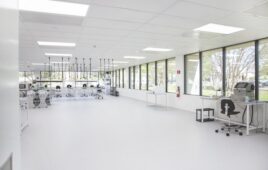
The Birck Nanotechnology Center (BNC) at Purdue University (Figure 7) was the first example of a higher education facility built to include both nanofabrication in a traditional cleanroom environment and a pharmaceutical grade cleanroom for molecular-based bioscience research. While both spaces are within the same building envelope, the engineering solutions and protocols used are customized for each of the unique environments.
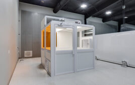
Before the NIST AML was built, NIST was trying to carry out cutting-edge research in laboratories built in the 1960s. The age and setup of the buildings caused a number of problems. For instance, small pieces of the fan belts on the air handling unit motor would flake off, travel down the ductwork, and get blown into the space, landing at some random location. Those little specks didn’t seem big, but when they landed on materials being fabricated at the nanoscale, they easily ruined experiments and samples. Dust particles also had a negative impact on their devices. The completed 8,000 s.f. nanofabrication facility (Figure 8) at the NIST Center for Nanoscale Science and Technology (CNST) is outfitted with Class 100 bay and chase cleanroom laboratories to operate as a shared-access user facility.


ELECTRICAL, ELECTRO MAGNETIC, AND RADIO FREQUENCY INTERFERENCE
Many of the instruments used by nanoscale researchers are highly sensitive to electrical and electromagnetic interference. Everything from a small fluctuation in the electrical power supply to electromagnetic interference (EMI) or radio frequency interference (RFI) can degrade research. At the outset of design, it is important to understand the specific requirements of the anticipated research in order to determine if EMI or RFI could be problematic.
Sometimes, the source of interference comes from forces outside the building and steps to limit it are required. An outside interference issue arose during early planning phases at the Center for Functional Nanomaterials (CFN) at Brookhaven National Laboratory (Figure 9). Concerns arose regarding the radio frequency (RF) emissions produced by a National Oceanic Atmospheric Administration (NOAA) Doppler radar located about a mile away. The site was tested specifically for that issue. Fortunately, the RF interference was low enough that it could be handled with local attenuation.
From an interior perspective, designers working to limit interference must be cognizant of how different types of labs are arranged. For example, labs that are particularly sensitive to electromagnetic interference should not be located near elevators or lab equipment that will produce strong electromagnetic fields. Certain systems necessary for maintaining the building must be taken into account. Transformers, rotating equipment, and pumps are examples of equipment required to keep basic building systems operational, but can also wreak havoc with laboratories. These essential building systems should be located where they are as benign as possible; and if necessary, local shielding can help create an environment appropriate for nanoscale research. Generally, when designing the interior of a nanoscale research facility, components known to cause interference should be segregated from research areas as much as possible.

RESEARCHERS ARE PEOPLE TOO!
Although the complex technical requirements discussed above are paramount, designers of these facilities also must evaluate and make provisions for human criteria. The present and future scientists who conduct research within the facility and also the public interface between the facility and the community at large are factors that cannot be overlooked.
It is crucial to remember that a technically “perfect” nanoscale laboratory will not function well if it is located in a facility where researchers do not want to work. Designing spaces for nanotechnology research is not only about how atoms, materials, and machines interact, it is also about how people interact. New ideas, new techniques, and new products are the result of people working with each other. Building designers can do a great deal to facilitate such interactions through the design of welcoming and comfortable spaces.
The NPL UK project illustrates how technical criteria can be isolated without isolating the scientists. In this project, various laboratories were designed as separate modules, yet the laboratories are connected through a series of bridges and connectors to shared spaces that allow for communication, collaboration and collective activities.
Likewise, the CINT project was built outside the perimeter of Sandia’s main campus and this allows researchers from different countries to collaborate with greater ease. The new building is secure, yet the protocols are less stringent than working within the perimeter of the main Sandia campus. The Brookhaven National Laboratory (BNL) Center for Functional Nanomaterials (CFN) contains highly sensitive laboratories and cleanrooms while providing ample opportunity for collaboration among scientists in strategically placed interaction areas. These interaction areas are also found in other buildings like the Purdue BNC. These areas are essential in fostering the impromptu communication inherent in any interdisciplinary research context (Figures 10 and 11).
Designers should not overlook the fact that buildings are often used as a recruitment tool. It is advantageous for a program to have a facility that will attract scientists. Designers should be aware of the importance of a building’s iconic image. Also, it is important to keep an eye toward the future needs and include spaces that will be easily adaptable for future growth and development.


PUBLIC INTERFACE
A building’s iconic image, helpful in attracting researchers, is also a tool for communicating the facility’s function to the public at large. The newly designed Joint School for Nanoscale and Nanoengineering (JSNN) in Greensboro, North Carolina (Figure 12) illustrates how extra care was devoted to use the building as a tool for communicating its function to the local community. The layout provides an openness and transparency that visually illustrates how cutting edge research has been incorporated as an investment in the local area. The layout allows the interior of the auditorium to be viewed by people driving on the nearby main road. In addition, the distribution of public space within the building provides maximum, yet safe exposure, to foster public awareness.


DESIGNING FOR THE UNKNOWN (THE FUTURE)
The Nanoscale Material Science and Engineering Building located at the University of Arkansas in Fayetteville (Figure 13) is an example of a facility designed with the future in mind. The University made its initial capital investment into a building that will allow them to grow their research program. In addition to flexibly designed laboratories and cleanrooms, the University created open shelled spaces that can be completed and adapted when more funding is available and future research parameters are ascertained.
Both the technical criteria and human criteria that culminate in the design of nanotech laboratories and facilities can present astounding complexities to the architects and engineers involved in creating the design. Even the best planning effort cannot predict perfectly how spaces will be used, or anticipate technological advancements that may dramatically affect space requirements.
Over time, spaces will be assigned to different researchers and programs, so architects and engineers should do what they can to build flexibility into any design. Just as interdisciplinary research is evolving and shaping the future of nanoscale research, architecture and building technologies in this context are also evolving. Traditional methods and models must yield to a new partnership between architects, engineers, nanoscale researchers, technical experts and institutions. By combining and integrating the perspectives and expertise of all parties involved, information and understanding will culminate to provide a sound basis for projecting and designing for the future.
Ahmad Soueid, AIA, LEED® AP, serves as HDR CUH2A’s National Director for the Advanced S+T Research program. He is an architect that provides creative design solutions and leadership on projects requiring critical environments. He has over two decades of focused experience on the design of technically challenging facilities and is a frequently invited speaker at international technical conferences. Mr. Soueid is considered a global leader in planning, design and construction of facilities established for nano-scale research. He can be reached at [email protected].