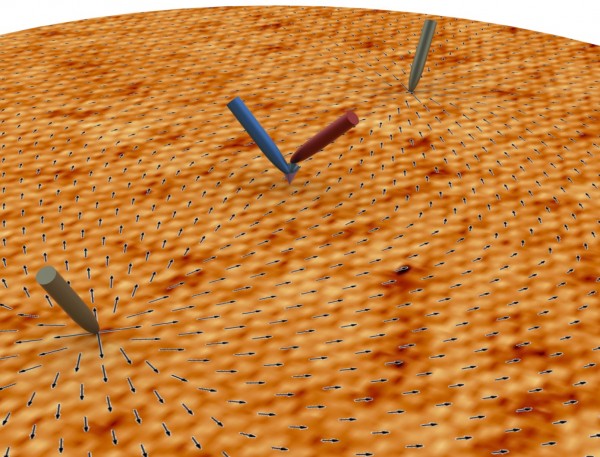
A new microscopy method developed by an ORNL-led team has four movable probing tips, is sensitive to the spin of moving electrons and produces high-resolution results. Using this approach, they observed the spin behavior of electrons on the surface of a quantum material. Saban Hus and An-Ping Li/Oak Ridge National Laboratory, U.S. Dept. of Energy
A new method that precisely measures the mysterious behavior and magnetic properties of electrons flowing across the surface of quantum materials could open a path to next-generation electronics.
Found at the heart of electronic devices, silicon-based semiconductors rely on the controlled electrical current responsible for powering electronics. These semiconductors can only access the electrons’ charge for energy, but electrons do more than carry a charge. They also have intrinsic angular momentum known as spin, which is a feature of quantum materials that, while elusive, can be manipulated to enhance electronic devices.
A team of scientists, led by An-Ping Li at the Department of Energy’s Oak Ridge National Laboratory, has developed an innovative microscopy technique to detect the spin of electrons in topological insulators, a new kind of quantum material that could be used in applications such as spintronics and quantum computing.
“The spin current, namely the total angular momentum of moving electrons, is a behavior in topological insulators that could not be accounted for until a spin-sensitive method was developed,” Li said.
Electronic devices continue to evolve rapidly and require more power packed into smaller components. This prompts the need for less costly, energy-efficient alternatives to charge-based electronics. A topological insulator carries electrical current along its surface, while deeper within the bulk material, it acts as an insulator. Electrons flowing across the material’s surface exhibit uniform spin directions, unlike in a semiconductor where electrons spin in varying directions.
“Charge-based devices are less energy efficient than spin-based ones,” said Li. “For spins to be useful, we need to control both their flow and orientation.”
To detect and better understand this quirky particle behavior, the team needed a method sensitive to the spin of moving electrons. Their new microscopy approach was tested on a single crystal of Bi2Te2Se, a material containing bismuth, tellurium and selenium. It measured how much voltage was produced along the material’s surface as the flow of electrons moved between specific points while sensing the voltage for each electron’s spin.
The new method builds on a four-probe scanning tunneling microscope—an instrument that can pinpoint a material’s atomic activity with four movable probing tips—by adding a component to observe the spin behavior of electrons on the material’s surface. This approach not only includes spin sensitivity measurements. It also confines the current to a small area on the surface, which helps to keep electrons from escaping beneath the surface, providing high-resolution results.
“We successfully detected a voltage generated by the electron’s spin current,” said Li, who coauthored a paper published by Physical Review Letters that explains the method. “This work provides clear evidence of the spin current in topological insulators and opens a new avenue to study other quantum materials that could ultimately be applied in next-generation electronic devices.”
Additional coauthors of the study titled, “Detection of the Spin-Chemical Potential in Topological Insulators Using Spin-Polarized Four-Probe STM,” include ORNL’s Saban Hus, Giang Nguyen, Wonhee Ko and Arthur Baddorf; X.-G. Zhang of the University of Florida; and Yong Chen of Purdue University.
This research was conducted at the Center for Nanophase Materials Sciences, a DOE Office of Science User Facility. The development of the novel microscopy method was funded by ORNL’s Laboratory Directed Research and Development program.