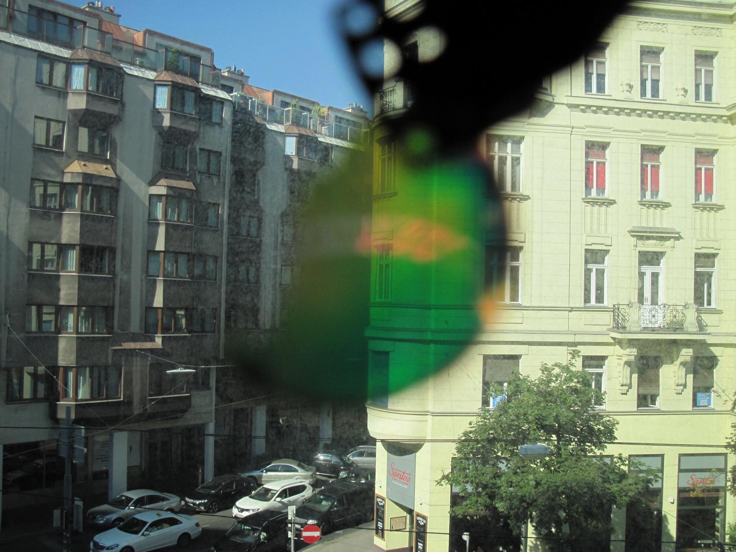
A structure designed in such a way that only green light is allowed to pass. Credit: TU Wien
Advancements in semiconductor technology could pave the way for micro-and-nanomachined sensors and electronic components.
Researchers from the TU Wien in Vienna have generated extremely fine porous structures with tiny holes—resembling a kind of sponge at the nano level—in semiconductors using monocrystalline silicon carbide, opening up new possibilities for the realization of tiny sensors or unusual optical and electronic components.
While there have already been experiments involving porous structures made from silicon, the researchers have developed a method to control the manufacture of porous silicon carbide (SiC), which has significant advantages over silicon.
Silicon carbide has greater chemical resistance than standalone silicon. It also can be used for more biological applications without additional coating.
The researchers integrated a special mirror that selectively reflects different colors of light into a SiC wafer by creating thin layers with a thickness of approximately 70 nanometers each, with different degrees of porosity.
“There is a whole range of exciting technical possibilities available to us when making a porous structure with countless nano holes from a solid piece of a semiconductor material,” Markus Leitgeb from the Institute of Sensor and Actuator Systems at TU Wien, said in a statement. “The porous structure influences the manner in which light waves are affected by the material.
“If we can control the porosity, this means we also have control over the optical refractive index of the material,” he added.
The new technology could be used for sensors, as the refractive index of tiny quantities of liquid can be measured using a porous semiconductor sensor, allowing a reliable distinction between different liquids.
The scientists are also the first to make certain areas of the SiC wafer porous in a highly localized manner, before depositing a new SiC layer over the porous areas. This causes the latter layers to collapse in a controlled manner, which produces microstructures and nanostructures that can also play a key role in sensor technology.
“Until now, silicon has been used for this purpose, a material with which we already have a lot of experience,” Ulrich Schmid, a professor from TU Wien, said in a statement.
However, structures made of silicon are attacked and rapidly destroyed in harsh environmental conditions like extreme heat or in alkaline solutions. Therefore, sensors made of silicon are often not suitable for biological or electrochemical applications.
To overcome these hurdles, the surface must first be cleaned and then partially covered with a thin layer of platinum. The silicon carbide is then immersed in an etching solution and exposed to UV light, in order to initiate the oxidation processes.
This causes a thin porous layer about one μm thick to form in the areas that are not coated with platinum. An electrical charge is then applied to be able to precisely set the porosity and the thickness of the subsequent layers. The first porous layer promotes the formation of the first pores when the electrical charge is applied.
“The porous structure spreads from the surface further and further into the interior of the material,” Leitgeb said. “By adjusting the electrical charge during this process, we can control what porosity we want to have at a given depth.”
It is possible to produce a complex layered structure of silicon carbide layers with higher and lower levels of porosity, which is finally separated from the bulk material by applying a high voltage pulse. The thickness of the individual layers can be selected so that the layered structure reflects certain wavelengths particularly well or allows certain light wavelengths to pass through, resulting in an integrated, color-selective mirror.
“We have thus demonstrated that our new method can be used to reliably control the porosity of silicon carbide on a microscopic scale,” Schmid said. “This technology promises many potential applications, from anti-reflective coatings, optical or electronic components and special biosensors, through to resistant supercapacitors.”
The study was published in APL Materials.


