Research & Development World

  • R&D World Home
  • Topics
    • Aerospace
    • Automotive
    • Biotech
    • Careers
    • Chemistry
    • Environment
    • Energy
    • Life Science
    • Material Science
    • R&D Management
    • Physics
  • Technology
    • 3D Printing
    • A.I./Robotics
    • Software
    • Battery Technology
    • Controlled Environments
      • Cleanrooms
      • Graphene
      • Lasers
      • Regulations/Standards
      • Sensors
    • Imaging
    • Nanotechnology
    • Scientific Computing
      • Big Data
      • HPC/Supercomputing
      • Informatics
      • Security
    • Semiconductors
  • R&D Market Pulse
  • R&D 100
    • 2026 R&D 100 Award Winners
    • 2026 Professional Award Winners
    • 2026 Special Recognition Winners
    • R&D 100 Awards Event
    • R&D 100 Submissions
    • Winner Archive
  • Resources
    • Research Reports
    • Digital Issues
    • Educational Assets
    • Subscribe
    • Video
    • Webinars
    • PharmSci360
    • Content submission guidelines for R&D World
  • Global Funding Forecast
  • Top Labs
  • Advertise
  • SUBSCRIBE

A New Approach to Simulating Nanoscale Heat Transfer

By R&D Editors | April 7, 2016

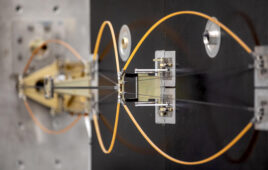
A research team led by Joe Feser in the Department of Mechanical Engineering at the University of Delaware has developed a new approach to simulating nanoscale heat transfer in materials. Image: Evan KrapeThermoelectric materials, which can directly and reversibly convert heat to electrical energy, are used in a variety of applications, including cooling of electronic devices and waste heat energy conversion.

A persistent challenge associated with thermoelectric materials is efficiency — if they could be designed to more efficiently convert heat into electricity, the door would be opened to a wide range of practical applications.

To make them more efficient, the materials must act like a thermal insulator while electronically behaving like a conductor — a feature not often found in natural materials.

A research group led by Joe Feser, assistant professor in the Department of Mechanical Engineering at the University of Delaware, is investigating the limits of heat transport using a suite of new tools for nanoscale thermal measurement and simulation, with an eye toward the creation of materials that are more thermoelectrically efficient.

One common strategy employed by his group is the use of nanoparticles to scatter heat-carrying vibrations, known as phonons. The team is developing tools to study phonon scattering so that the size, shape, and composition of nanoparticles can be optimized for thermoelectric applications.

Feser and doctoral student Rohit Kakodkar recently reported a new approach to that problem in a paper, “A Framework for Solving Atomistic Phonon-Structure Scattering Problems in the Frequency Domain Using Perfectly Matched Layer Boundaries,” in the Journal of Applied Physics.

The new framework significantly reduces the amount of computational power needed to simulate phonon scattering and greatly increases the maximum size of the systems that can be studied using computers.

Feser explains that continuum mechanics models — which, for the sake of efficiency, ignore the fact that matter is made up of atoms — are traditionally used to explain phenomena like phonon scattering. However, while this approach is accurate enough on length scales greater than the distance between atoms, it may not be effective in characterizing the behavior of nanometer-length waves, which are often the wavelengths involved in heat transport.

The obvious solution is to have simulations that include an equation for each individual atom and track the behavior over an extended period of time, but that’s where the computational logjam occurs. Traditional techniques like molecular dynamics are too slow to simulate scattering for every heat-carrying vibration separately, and other existing techniques are limited in their ability to simulate large systems.

The atomistic model developed by Feser and Kakodkar can solve for a large number of atoms at a time. “Basically what we’ve done is remove the unnecessary physics and embed facts we already know about the solutions into the solution procedure,” Feser says.

Another important use for the new tool is that it has enabled researchers to settle longstanding controversies about how to describe the physics of phonons encountering interfaces — that is, whether they travel across coherently or scatter diffusely — and especially how disorder changes that. The framework also has the advantage that it can be scaled up for use with supercomputers, which are seeing increased use for complex simulations.

Ultimately, the goal is to have precise control over the design of new materials at the level of their tiniest constituents.

“The design of new materials that push the limits of achievable transport properties — i.e., thermal conductivity, interface conductance, heat capacity, and thermoelectric power factor — will enable the development of new device technologies based on these materials,” Feser says.

Source: University of Delaware 
Related Articles Read More >

A researcher handles a prismatic battery cell on PNNL’s manufacturing line.
DOE’s BattMan brings four national labs together to de-risk battery scale-up
INL’s $60 million nuclear AI project will spend the first year testing where AI agents can help and where they might hurt 
The Space Systems Division (05)-developed Parallelogram Synchronized Truss Assembly (PaSTA), seen Aug. 12, 2025, is a mechanism that will be integrated into the Life-Extension In-orbit Servicer (LEXI) and Astroscale Prototype Servicer for Refueling (APS-R) spacecrafts.
One SwRI R&D 100 winner turns buckled fiberglass into a spacecraft truss. The other models freight rail with 900 hours of BNSF field data
Inside the Lab: NETL’s Oil and Gas Center of Excellence focuses on technologies to enhance production   
rd newsletter
EXPAND YOUR KNOWLEDGE AND STAY CONNECTED
Get the latest info on technologies, trends, and strategies in Research & Development.

R&D World Digital Issues

Fall 2026 issue

Browse the most current issue of R&D World and back issues in an easy to use high quality format. Clip, share and download with the leading R&D magazine today.

R&D 100 Awards
Research & Development World
  • Subscribe to R&D World Magazine
  • Sign up for R&D World’s newsletter
  • Contact Us
  • About Us
  • Drug Discovery & Development
  • Pharmaceutical Processing
  • Global Funding Forecast

Copyright © 2026 Arrowfly LLC. All Rights Reserved. The material on this site may not be reproduced, distributed, transmitted, cached or otherwise used, except with the prior written permission of Arrowfly
Privacy Policy | Advertising | About Us

Search R&D World

  • R&D World Home
  • Topics
    • Aerospace
    • Automotive
    • Biotech
    • Careers
    • Chemistry
    • Environment
    • Energy
    • Life Science
    • Material Science
    • R&D Management
    • Physics
  • Technology
    • 3D Printing
    • A.I./Robotics
    • Software
    • Battery Technology
    • Controlled Environments
      • Cleanrooms
      • Graphene
      • Lasers
      • Regulations/Standards
      • Sensors
    • Imaging
    • Nanotechnology
    • Scientific Computing
      • Big Data
      • HPC/Supercomputing
      • Informatics
      • Security
    • Semiconductors
  • R&D Market Pulse
  • R&D 100
    • 2026 R&D 100 Award Winners
    • 2026 Professional Award Winners
    • 2026 Special Recognition Winners
    • R&D 100 Awards Event
    • R&D 100 Submissions
    • Winner Archive
  • Resources
    • Research Reports
    • Digital Issues
    • Educational Assets
    • Subscribe
    • Video
    • Webinars
    • PharmSci360
    • Content submission guidelines for R&D World
  • Global Funding Forecast
  • Top Labs
  • Advertise
  • SUBSCRIBE