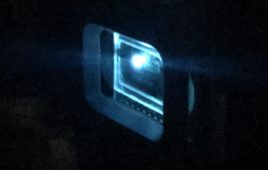
Laser writing of individual nitrogen-vacancy defects in diamond with near-unity yield. Image: Oxford University
“Quantum technologies” utilize the unique phenomena of quantum superposition and entanglement to encode and process information, with potentially profound benefits to a wide range of information technologies from communications to sensing and computing.
However, a major challenge in developing these technologies is that the quantum phenomena are very fragile, and only a handful of physical systems have been identified in which they survive long enough and are sufficiently controllable to be useful. Atomic defects in materials such as diamond are one such system, but a lack of techniques for fabricating and engineering crystal defects at the atomic scale has limited progress to date.
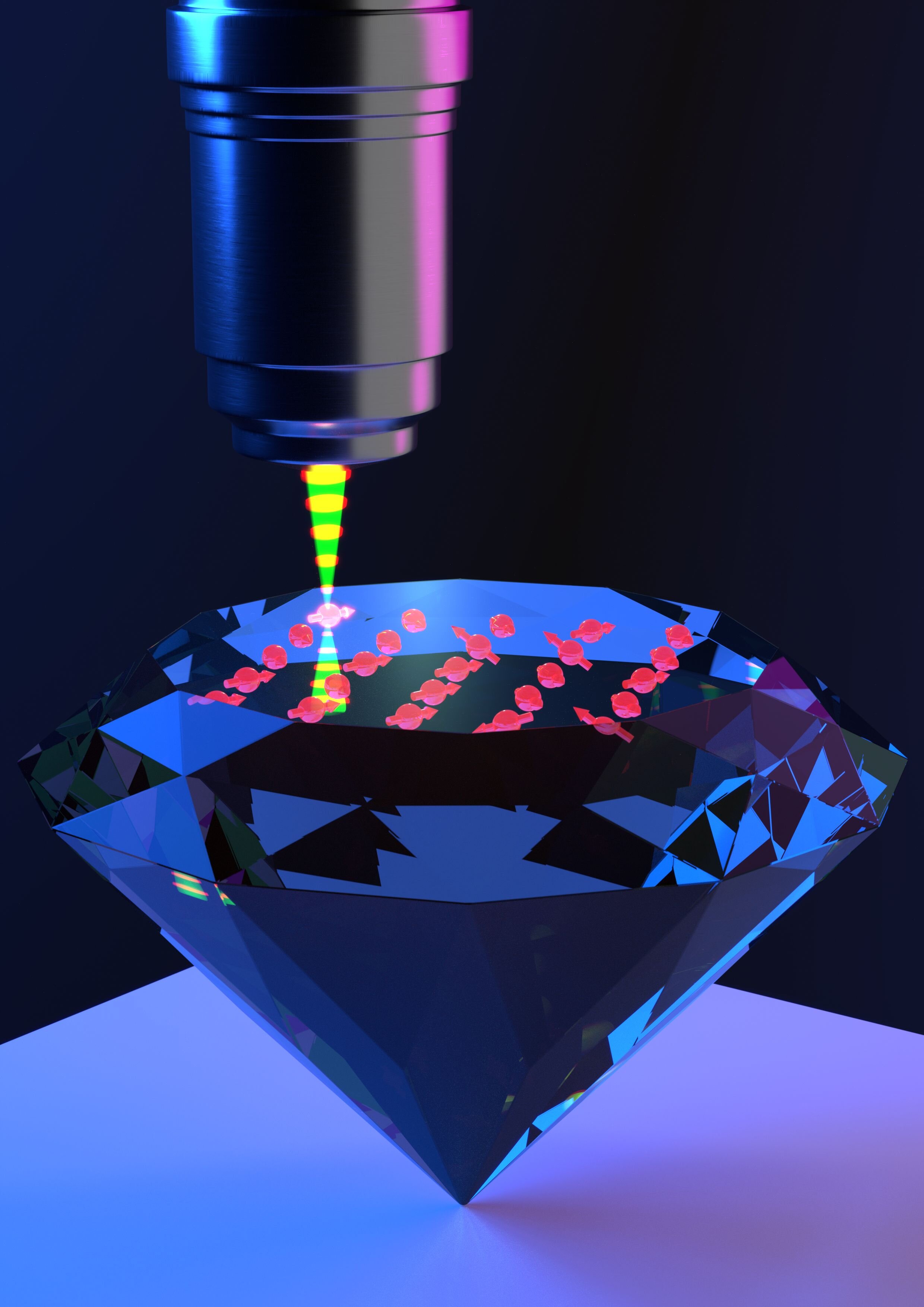
A team of scientists demonstrate, in a paper published in Optica, the success of the new method to create particular defects in diamonds known as nitrogen-vacancy (NV) color centers. These comprise a nitrogen impurity in the diamond (carbon) lattice located adjacent to an empty lattice site or vacancy.
The NV centers are created by focusing a sequence of ultrafast laser pulses into the diamond, the first of which has an energy high enough to generate vacancies at the center of the laser focus, with subsequent pulses at a lower energy to mobilize the vacancies until one of them binds to a nitrogen impurity and forms the required complex.
The new research was carried out by a team led by Prof Jason Smith in the Department of Materials, University of Oxford, and Dr. Patrick Salter and Prof Martin Booth in the Department of Engineering Science, University of Oxford, in collaboration with colleagues at the University of Warwick. It took place within the research program of NQIT, the Quantum Computing Technology Hub of the UK Quantum Technologies Programme, with support from DeBeers UK who supplied the diamond sample.
The scientists’ new method involves a sensitive fluorescence monitor being employed to detect light emitted from the focal region, so that the process can be actively controlled in response to the observed signal. By combining local control and feedback, the new method facilitates the production of arrays of single NV centers with exactly one color center at each site—a key capability in building scalable technologies. It also allows precise positioning of the defects, important for the engineering of integrated devices. The rapid single-step process is easily automated with each NV center taking only seconds to create.
Professor Martin Booth says: “Color centers in diamond offer a very exciting platform for developing compact and robust quantum technologies, and this new process is a potential game-changer in the engineering of the required materials. There is still more work to do in optimizing the process, but hopefully this step will help to accelerate delivery of these technologies.”
The scientists believe that this method might ultimately be used to fabricate centimeter-sized diamond chips containing 100,000 or more NV centers as a route towards the “holy grail” of quantum technologies, a universal fault-tolerant quantum computer.
Professor Jason Smith says: “The first quantum computers are now starting to emerge but these machines, impressive as they are, only scratch the surface of what might be achieved and the platforms being used may not be sufficiently scalable to realize the full power that quantum computing has to offer. Diamond color centers may provide a solution to this problem by packing high densities of qubits onto a solid state chip, which could be entangled with each other using optical methods to form the heart of a quantum computer. The ability to write NV centers into diamond with a high degree of control is an essential first step towards these and other devices.”