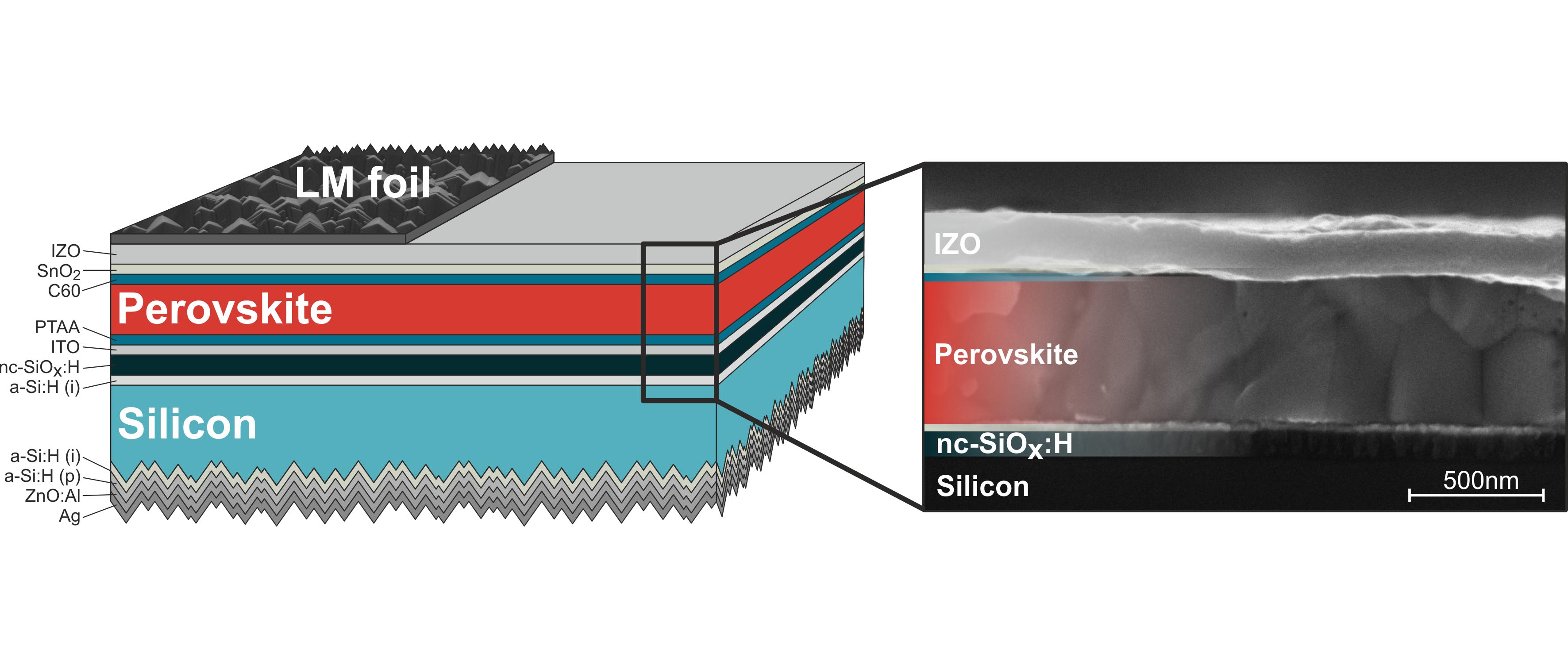
Above the perovskite layer, a structured polymer film provides better light capture. Image: HZB
Using microstructured layers, a Helmholtz-Zentrum Berlin team has been able to increase the efficiency of perovskite-silicon tandem solar cells, achieving 25.5 percent, which is the highest published value to date.
At the same time, computational simulations were utilized to investigate light conversion in various device designs with different nanostructured surfaces. This enabled optimization of light management and detailed energy yield analyses.
The study has now been published in Energy & Environmental Science.
Tandem solar cells made of silicon and metal halide perovskite compounds can convert a particularly large portion of the solar spectrum into electrical energy. However, part of the light is reflected and is thus lost for purposes of energy conversion.
Using nanostructures, the reflection can be reduced significantly ensuring that the solar cell captures more light.
For example, pyramid-shaped microfeatures can be etched into silicon. However, these features cause microscopic roughness in the silicon surface, making it no longer suitable as a substrate for deposition of extremely thin perovskite layers. This is because perovskites are normally deposited to a polished wafer using solution processing to form an extremely thin film, much thinner than the pyramidal features. A rough-etched silicon surface layer therefore prevents formation of a uniform conformal layer.
A team headed by HZB physicist Steve Albrecht has investigated an alternative approach of light management with textures in tandem solar cells. The team fabricated an efficient perovskite/silicon tandem device whose silicon layer was etched on the backside. The perovskite layer could be applied by spincoating onto the smooth front-side of the silicon.
The team afterwards applied a polymer light management (LM) foil to the front-side of the device. This enabled processing of a high-quality perovskite film on a flat surface, while still benefiting from the front-side texture.
“In this way, we succeeded in considerably improving the efficiency of a monolithic perovskite-silicon heterojunction tandem cell from 23.4 percent to 25.5 percent,” says Marko Jošt, first author of the study and postdoctoral fellow in Albrecht’s team.
In addition, Jošt and colleagues have developed a sophisticated numerical model for complex 3D features and their interaction with light. This enabled the team to calculate how different device designs with textures at various interfaces affect efficiency.
“Based on these complex simulations and empirical data, we believe that an efficiency of 32.5 percent can realistically be achieved — if we succeed to incorporate high quality perovskites with a band gap of 1.66 eV,” says Jošt.
Team leader Albrecht adds: “Based on real weather data, we were able to calculate the energy yield over the course of a year — for the different cell designs and for three different locations.”
In addition, the simulations show that the LM foil on the front-side of the solar cell device is particularly advantageous under diffuse light irradiation, i.e. not only under perpendicularly incident light. Tandem solar cells with the new LM foil could therefore also be suitable for incorporation in building-integrated photovoltaics (BIPV), opening up huge new areas for energy generation from large skyscraper facades.
Source: Helmholtz-Zentrum Berlin