Tucked away in the Physics Building, a sophisticated new tool that can make extremely small objects — too small to see with the eye alone — will mean big things for science across the Colorado State University campus.
It’s called a maskless photolithography system, and it allows prototyping objects 100 times smaller than the width of a human hair.
The $230,000 instrument was brought to campus earlier this year, thanks to a National Science Foundation Major Research Instrumentation grant secured by faculty members in the Department of Physics, and cost-matching provided by Colorado Higher Education Competitive Research Authority.
With more than 30 students and other users now trained on the state-of-the-art machine, organizers hope it will provide a valuable resource for researchers, from physicists and engineers to life scientists.
Photolithography, which roughly means “writing with light,” is a workhorse technology most significant to the semiconductor industry, which brings us the microprocessors and circuits in our computers, cell phones and coffeemakers.
In photolithography, small, precise patterns are transferred onto a surface using strong ultraviolet light. These patterns are exposed onto a thin plastic coating called photoresist. An ultraviolet laser spot scans over the surface, turning a light on and off, to write the desired pattern.
It’s this technology that allows Intel and other chip makers to design and build circuits like the Haswell Chip, a microprocessor whose smallest components are just a few nanometers wide. A nanometer is one-billionth of a meter.
CSU’s new photolithography tool is capable of making objects down to a resolution of about 600 nanometers, or 0.6 microns, employing the same basic technology.
Besides its nanoscale capabilities, CSU’s new tool also brings users speed, consistency and repeatability. Other types of photolithography systems use a photomask, a master pattern that first needs to be made, then transferred onto the desired surface. CSU’s new system is “maskless,” so that step is not required.
“Our new system is great for rapid prototyping, adjusting features, and tuning patterns,” says Kristen Buchanan, associate professor of physics and grant principal investigator.
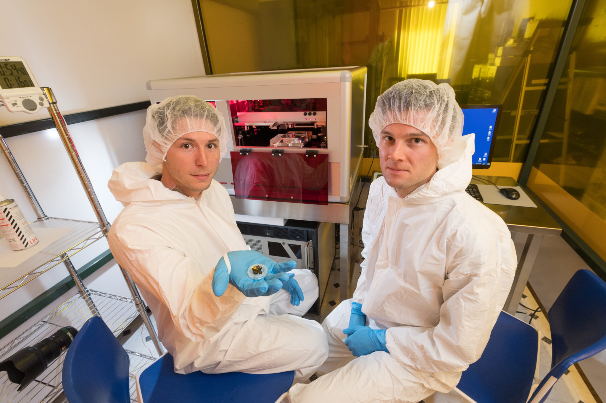
Physics Ph.D. students Weston Maughan and Gus DeMann with the maskless photolithography tool. Maughan is holding gold electrical contacts patterned on a silicon wafer. Image: John Eisele
The new system complements existing facilities available on campus, including an electron beam lithography machine in the Central Instrument Facility. While electron beam lithography can write structures down to a few nanometers, it’s not as useful for writing things with large features due to time and cost constraints.
Users of the new system so far have come from engineering, physics and biological sciences, showcasing its possibilities.
“We hope the versatility of the tool will inspire some projects we never even envisioned,” Buchanan says.
“This new machine has already opened up a lot of doors, with the sheer number of different devices we’ve made since it came in April,” says Stuart Field, associate professor of physics, who co-wrote the NSF grant with Buchanan and Mingzhong Wu, professor of physics.
“We can just try all sorts of things we wouldn’t have been able to attempt before.”
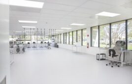
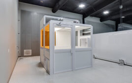
The photolithography system is housed in a cleanroom in the Physics Building, a specially designated space with HEPA filters and temperature controls to protect delicate samples.
Over the summer, physics graduate students Gus DeMann and Weston Maughan helped prepare the space for the new machine. DeMann has been principally responsible for providing training and guidance for new users.
In his own research in Field’s lab, DeMann is using the photolithography tool to create prototypes of low-temperature superconductors. He is fabricating granular aluminum in various shapes to study the strange behavior of magnetic fields in superconductors at extremely cold temperatures.
“A huge part of what makes this instrument so special is the accessibility and flexibility it affords its users,” DeMann says.
For example, if he has designed a sensor that isn’t working well, “the next day, I can go in, and change the design, and it’s done … the machine allows you to work in a way that’s affordable and efficient, without spending too much money or time.”
Maughan, also in Field’s group, has made superconducting nanowires using many layers of lithographic steps — already pushing the limits of what the machine can do.
The tool has also opened up new avenues for research in the lab of Professor Tom Chen, in the Department of Electrical and Computer Engineering, where Ph.D. student Ming-Hao Cheng has been using the lithography machine to make custom biosensors to monitor the metabolic rates of cells.
Previously he had used a printed mask and UV light to make devices, which worked pretty well for single-layer patterning, but fell apart at smaller, multi-layer scales.
The new laser writer, Cheng says, has cut down his turnaround time tremendously, allowing him to make incremental changes quickly.
“Now I don’t need to send my design to a photomask company, spend $100 and get the mask one week later,” he says.
The machine is open to any and all interested users.
Source: Colorado State University