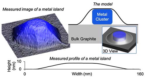
Ames Laboratory and Northeastern University developed and validated a model that predicts the shape of metal nanoparticles blanketed by 2D material. The top blanket of graphene resists deformation, “squeezing” downward on the metal nanoparticle and forcing it to be extremely low and wide.
In a collaboration between the U.S. Department of Energy’s Ames Laboratory and Northeastern University, scientists have developed a model for predicting the shape of metal nanocrystals or “islands” sandwiched between or below two-dimensional (2D) materials such as graphene. The advance moves 2D quantum materials a step closer to applications in electronics.
Ames Laboratory scientist are experts in 2D materials, and recently discovered a first-of-its-kind copper and graphite combination, produced by depositing copper on ion-bombarded graphite at high temperature and in an ultra-high vacuum environment. This produced a distribution of copper islands, embedded under an ultra-thin “blanket” consisting of a few layers of graphene.
“Because these metal islands can potentially serve as electrical contacts or heat sinks in electronic applications, their shape and how they reach that shape are important pieces of information in controlling the design and synthesis of these materials,” said Pat Thiel, an Ames Laboratory scientist and Distinguished Professor of Chemistry and Materials Science and Engineering at Iowa State University.
Ames Laboratory and Northeastern University developed and validated a model that predicts the shape of metal nanoparticles blanketed by 2D material. The top blanket of graphene resists deformation, “squeezing” downward on the metal nanoparticle and forcing it to be extremely low and wide.
Ames Laboratory scientists used scanning tunneling microscopy to painstakingly measure the shapes of more than a hundred nanometer-scale copper islands. This provided the experimental basis for a theoretical model developed jointly by researchers at Northeastern University’s Department of Mechanical and Industrial Engineering and at Ames Laboratory. The model served to explain the data extremely well. The one exception, concerning copper islands less than 10 nm tall, will be the basis for further research.
“We love to see our physics applied, and this was a beautiful way to apply it,” said Scott E. Julien, Ph.D. candidate, at Northeastern. “We were able to model the elastic response of the graphene as it drapes over the copper islands, and use it to predict the shapes of the islands.”
The work showed that the top layer of graphene resists the upward pressure exerted by the growing metal island. In effect, the graphene layer squeezes downward and flattens the copper islands. Accounting for these effects as well as other key energetics leads to the unanticipated prediction of a universal, or size-independent, shape of the islands, at least for sufficiently large islands of a given metal.
“This principle should work with other metals and other layered materials as well,” said Research Assistant, Ann Lii-Rosales. “Experimentally we want to see if we can use the same recipe to synthesize metals under other types of layered materials with predictable results.”
The research is further discussed in the paper, “Squeezed Nanocrystals: Equilibrium Configuration of Metal Clusters Embedded Beneath the Surface of a Layered Material,” authored by Scott E. Julien, Ann Lii-Rosales, Kai-Tak Wan, Yong Han, Michael C. Tringides, James W. Evans, and Patricia A. Thiel; and published in Nanoscale.
The research was a collaboration between Ames Laboratory and Northeastern University. Work at Northeastern University was supported by the National Institute of Standards and Technology (NIST), a national facility operated under the U.S. Department of Commerce.
Work at Ames Laboratory was supported primarily by the U.S. Department of Energy Office of Science. This work was also supported in part by a grant of computer time at the National Energy Research Scientific Computing Centre (NERSC), a DOE Office of Science User Facility.


