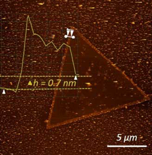
Atomic force microscopy image of two-dimensional tungsten disulfide grown with the furnace. Image: Boise State University
A research group at Boise State University led by Assistant Professor David Estrada of the Micron School of Materials Science and Engineering has released the open-source design of a chemical vapor deposition (CVD) system for two-dimensional (2D) materials growth, an advance which could lower the barrier of entry into 2D materials research and expedite 2D materials discovery and translation from the benchtop to the market.
Two-dimensional materials are a class of materials that are one to a few atoms thick. The pioneering work of Nobel Laureates Andre Geim and Konstantin Novoselov in isolating and measuring the physical properties of graphene—a 2D form of carbon arranged in a hexagonal crystal structure—ignited the field of 2D materials research.
While 2D materials can be obtained from bulk van der Waals crystals (e.g. graphite and MoS2) using a micromechanical cleavage approach enabled by adhesive tapes, the community quickly realized that unlocking the full potential of 2D materials would require advanced manufacturing methods compatible with the semiconductor industry’s infrastructure.
Chemical vapor deposition is a promising approach for scalable synthesis of 2D materials—but automated commercial systems can be cost prohibitive for some research groups and startup companies. In such situations students are often tasked with building custom furnaces, which can be burdensome and time consuming. While there is value in such endeavors, this can limit productivity and increase time to degree completion.
A recent trend in the scientific community has been to develop open-source hardware and software to reduce equipment cost and expedite scientific discovery. Advances in open-source 3-dimensional printing and microcontrollers have resulted in freely available designs of scientific equipment ranging from test tube holders, potentiostats, syringe pumps and microscopes. Estrada and his colleagues have now added a variable pressure chemical vapor deposition system to the inventory of open-source scientific equipment.
“As a graduate student I was fortunate enough that my advisor was able to purchase a commercial chemical vapor deposition system which greatly impacted our ability to quickly grow carbon nanotubes and graphene. This was critical to advancing our scientific investigations,” said Estrada. “When I read scientific articles I am intrigued with the use of the phrase “custom-built furnace” as I now realize how much time and effort graduate students invest in such endeavors.”
The design and qualification of the furnace was accomplished by lead authors Dale Brown, a former Micron School of Materials Science and Engineering graduate student, and Clinical Assistant faculty member Lizandra Godwin, with assistance from the other co-authors.
The results of their variable pressure CVD system have been published in PLoS One (“Open-source automated chemical vapor deposition system for the production of two- dimensional nanomaterials”) and include the parts list, software drivers, assembly instructions and programs for automated control of synthesis procedures. Using this furnace, the team has demonstrated the growth of graphene, graphene foam, tungsten disulfide and tungsten disulfide—graphene heterostructures.
“Our goal in publishing this design is to alleviate the burden of designing and constructing CVD systems for the early stage graduate student,” said Godwin. “If we can save even a semester of time for a graduate student this can have a significant impact on their time to graduation and their ability to focus on research and advancing the field.”
“We hope others in the community can improve on our design by incorporating open-source software for automated control of 2D materials synthesis,” said Estrada. “Such an improvement could further reduce the barrier to entry for 2D materials research.”