In the 1940s, scientists first explained how materials can deform plastically by atomic-scale line defects called dislocations. These defects can be understood as tiny carpet folds that can move one part of a material relative to the other without spending a lot of energy. Many technical applications are based on this fundamental process, such as forging, but we also rely on the power of dislocations in our everyday life: in the crumple zone of cars dislocations protect lives by transforming energy into plastic deformation.
Friedrich-Alexander-Universität Erlangen-Nürnberg (FAU) researchers have now found a way of manipulating individual dislocations directly on the atomic scale — a feat only dreamt of by materials scientists. Using advanced in situ electron microscopy the researchers in Professor Erdmann Spiecker’s group opened up new ways to explore the fundamentals of plasticity and reported their findings in the leading scientific journal Science Advances.
In 2013 an interdisciplinary group of researchers at FAU found the presence of dislocations in bilayer graphene — a groundbreaking study that was published in the prestigious journal Nature. The line defects are contained between two flat, atomically thin sheets of carbon — the thinnest interface where this is possible.
“When we found the dislocations in graphene we knew that they would not only be interesting for what they do in the specific material, but also that they could serve as an ideal model system to study plasticity in general,” Spiecker explains. To continue the story his team of two doctoral candidates knew that just seeing the defects would not be enough: they needed a way to interact with them.
A powerful microscope is needed to see dislocations. The researchers from Erlangen are specialists in the field of electron microscopy and are constantly thinking of ways to expand the technique.
“During the last three years we have steadily expanded the capabilities of our microscope to function like a workbench on the nanoscale,” says Peter Schweizer. “We can now not only see nanostructures but also interact with them, for example by pushing them around, applying heat or an electrical current.”
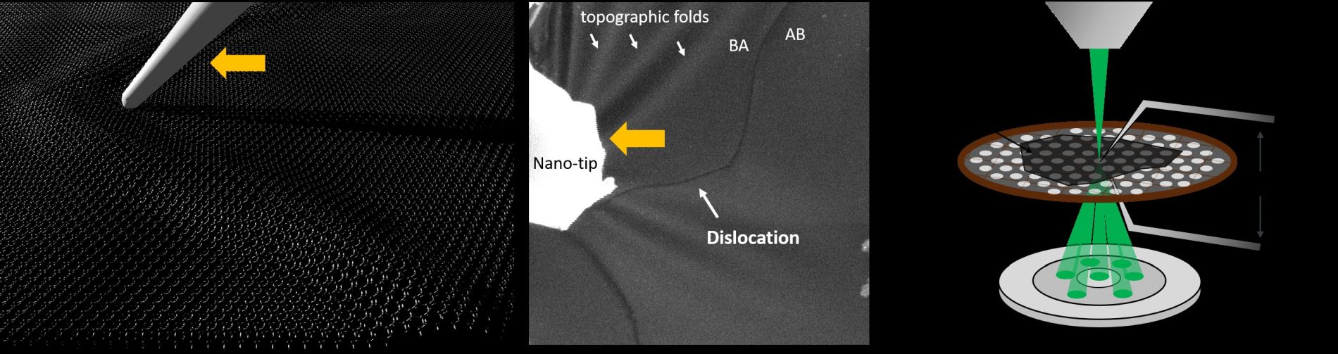
Plasticity in materials is mainly carried by atomic-scale line defects called dislocations. These dislocations can now be directly controlled by a nano-tip (schematic shown on the left, real image in the middle) as researchers from Erlangen have found. The manipulation is performed inside an electron microscope enabling the concurrent imaging of the defects and manipulation with ultra-sensitive robot arms (schematic shown on the right). Image: Peter Schweizer
At the core of this instrument are small robot arms that can be moved with nm-precision. These arms can be outfitted with very fine needles that can be moved onto the surface of graphene; however, special input devices are needed for high-precision control.
“Students often ask us what the gamepads are for,” says Christian Dolle and laughs, “but of course they are purely used for scientific purposes.”
At the microscope where the experiments were conducted, there are many scientific instruments — and two video game controllers.
“You can’t steer a tiny robot arm with a keyboard, you need something that is more intuitive,” Christian explains. “It takes some time to become an expert, but then even controlling atomic scale line defects becomes possible.”
One thing that surprised the researchers at the beginning was the resistance of graphene to mechanical stress. “When you think about it, it is just two layers of carbon atoms — and we press a very sharp needle into that,” says Schweizer. For most materials that would be too much, but graphene is known to withstand extreme stresses. This enabled the researchers to touch the surface of the material with a fine tungsten tip and drag the line defects around. “When we first tried it, we didn’t believe it would work, but then we were amazed at all the possibilities that suddenly opened up.”
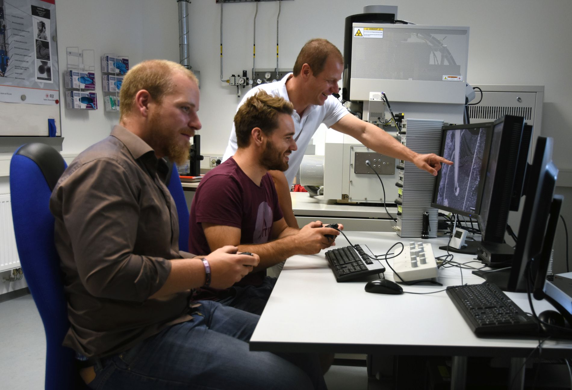
Research can be fun: Christian Dolle, Peter Schweizer and Prof. Spiecker (from left to right) at their “nano workbench.” Image: Mingjian Wu
Using this technique the researchers could confirm long-standing theories of defect interactions as well as find new ones. “Without directly controlling the dislocation it would not have been possible to find all these interactions!”
One of the decisive factors for the success was the excellent equipment at FAU and its Centre for Nanoanalysis and Electron Microscopy (CENEM). “Without having state-of-the art instruments and the time to try something new this would not have been possible.”
Spiecker acknowledges the excellent facilities in Erlangen which he hopes will continue to evolve in the future. “It’s important to grow with new developments, and try to broaden the techniques you have available.”
Additionally, the close interdisciplinary collaboration that FAU is known for acted as a catalyst for the new approach. The highly synergistic environment is strongly supported by the German Research Foundation (DFG) within the framework of a collaborative research center “Synthetic carbon allotropes” (SFB 953) and the research training group “in situ microscopy” (GRK1896) — a fertile ground for further exciting discoveries.