A standard sounds easy to meet, but semiconductor manufacturers know cleanroom standards are anything but run-of-the-mill. The heavy price of lost product demands that custodial partners provide service as exceptional as the wafers you’re producing. Safeguarding profit margins means particle control practices must be rigorously compliant, expertly effective, and above all, 100 percent integrated with your cleanroom protocols.
A current look at IC device manufacturing states 75 percent of yield losses happen because of contamination. When contamination is found, it’s often smart risk management to scrap an entire batch — easily a loss of millions of dollars. The possibility of expensive investigations, downtime, and loss of client and customer confidence only compound the loss of product and productivity.
Untangling risk and cost
The pressure of production goals can also be a source of risk. As nanometer measurements have thinned in the semiconductor world, the prospect of thinning profit margins has put decision-makers up and down the supply chain to the test. If cleaning is compromised in favor of pushing production goals, risk of contamination and risk to those same production goals can rise.
Expert cleanroom cleaning takes that tension off the table by protecting production with cost-effective, efficient, and most importantly results-driven service. In addition, proper cleaning not only protects against the high costs of lost product, but efficient cleaning process can affect day-to-day profitability. A 2017 survey by Controlled Environments noted 36 percent of cleanroom cleaning tasks still reside with cleanroom production workers themselves.1 A Gallup statistic states that people using their strengths are six times more likely to be engaged at work, so it’s clear that high-skill workers asked to take on cleaning tasks may become disengaged. If cleaning tasks are deprioritized for other responsibilities, the chance of contamination rises. An expert in cleanroom custodial is free to focus on cleaning as a core task and take pride in their work.
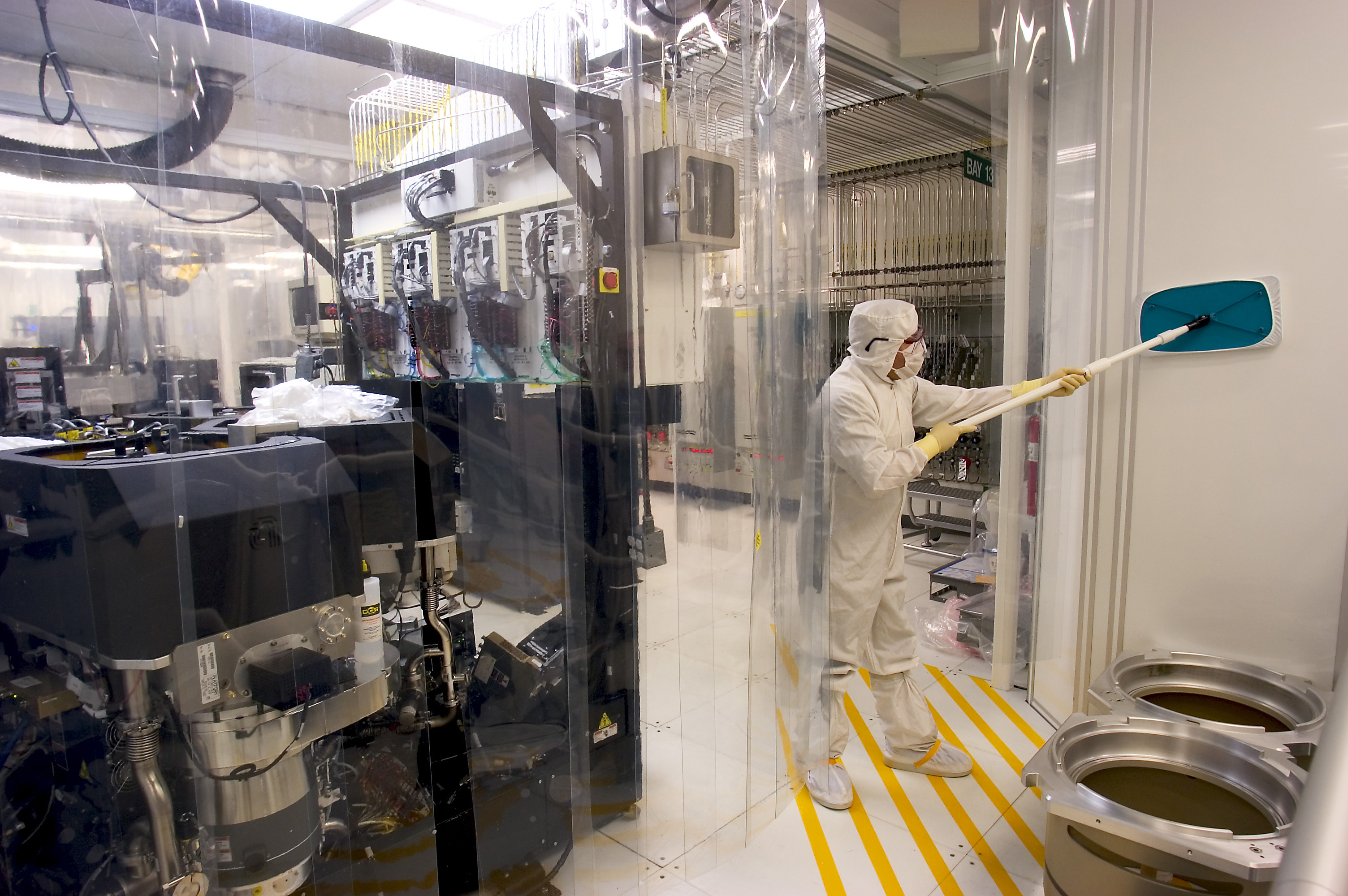
Semiconductor manufacturers know cleanroom control practices must be rigorously compliant, expertly effective, and above all, 100 percent integrated with your cleanroom protocols. Image: ABM
Contamination happens
No matter how careful people are, contaminants are introduced. Tools or equipment in the room will generate or collect particulates that must be captured before they can migrate to sensitive surfaces. Protecting the integrity of a cleanroom depends on proper cleaning to reduce those contaminants.
The biggest source of contamination is people, so training on procedure and protocol is the largest targeted objective. To protect product and uptime, cleaning needs to perfectly mesh with your SOPs, safety protocols, and production schedule. These five risks must all be diligently addressed:
• Unapproved cleaning solutions
• Improper cleaning technique
• Improper hygiene
• Introduction of foreign materials
• Improper gowning
While a service provider should have clear solutions for controlling all these risk factors, proper gowning technique cannot be stressed enough. As semiconductor professionals know, gowning can begin to feel repetitive, and any repetitive process requires diligent attention to ensure compliance. Industry experts in cleanroom custodial know they need technicians to understand the cost of subverting this key process. A gowning sequence needs to be exactly adhered to, every time.
EHS first!
While contamination control should always be a primary focus, the simple fact is that environmental health and safety (EHS) concerns can cause an immediate stop in production. In semiconductor fabs, production workers or cleaners may work near toxic substances. Custodians must be trained in labels for chemicals and signage used in and around the fab. There may also be special procedures for item disposal, such as color-coded bags for cleaning wipes that may have been exposed to certain solvents. Technicians need to understand all critical signage, such as emergency-off (EMO) switches, lock out and tag out, arc flash boundaries, and more.
High ceilings in many fabs require rules for elevated spaces. When cleaning underfloor, issues with confined spaces arise and protocols must be observed for placing signs around the area. It’s not as obvious as a construction worker’s exposure to heat stroke, but custodians should know to drink enough water to counteract their exposure to the excessive aridity of cleanrooms.
Humans being what we are
Cleaners must comply with control regimens to keep contaminants out. These rules are over and above what a layman might expect of an employee. Cleanroom cleaners must be properly vetted and training must install a level of respect for regimens that empower continual, self-regulated compliance. For instance, cleanroom protocols may prohibit a technician with sunburn from entering due to the increased risk of flaking skin particles. That takes a standard of care on the part of employees that’s anything but standard. No smoking is allowed, and neither is gum. Hygiene procedures and specific clothing are required. A service partner’s ability to provide a pool of sufficiently vetted and trained labor that is able to meet key behavioral expectations throughout evolving semiconductor production needs is critical. In the event of a super-clean event, a fab may require a service partner to provide three times the workers required by any normal shift.
Wiping out costs
Meticulous work requires proper cleaning techniques, which can be very repetitive. A service partner trains their employees to use the repetitive nature of tasks to not only control contaminants but to produce efficiency.
A cleanroom can spend literally millions on wipes alone. Proper techniques can maximize the use of wipe surface to help control those costs. Efficient cleaning practices such as wiping patterns can control particles while also reducing waste.
Documentation is more than a checkmark
On a basic level, compliance with standards requires that tasks be documented. If cleaning isn’t recorded, the cost of that cleaning is wasted — and, worse, the cost of repeating that cleaning may become a necessity to ensure standing operating procedures are met.
Training in special recordkeeping, such as cleanroom notebooks, may be required. Beyond the need to check off a few boxes, cleanroom cleaning requires a team that steps up to the responsibility of integrating their practices with the production team. Authorizations for needed equipment must be planned for to avoid delays. If work is needed in a certain bay, or a certain chase, notices must be given to affected tool operators.
Documented schedules require proactive attention y the cleaning team. Custodians must be prepared to work in and around an environment that could be live 24 hours a day, and prepared with the proper sign-offs to meet cleaning needs on time. All safety and compliance documentation must be completed in a timely manner so that all parties know that what needs to happen will happen when it’s supposed to happen — so that efforts are focused on protecting yield at all times.
Meeting the standards, both efficiently and cost-effectively
Semiconductor manufacturers deserve assurance from their cleanroom custodial partners. The standard operating procedures so carefully developed for billion-dollar facilities depend on principled service delivery to achieve them. To help safely meet standards and control costs, custodial partners need to reliably produce extraordinarily precise service repeatedly and efficiently. The key to that extraordinary reliability is vetted, highly trained personnel able to conform precisely to protocols and help avoid the costly impact of scrapped wafer.
References
1. Cleanroom Trends and Salary Survey, Controlled Environments, July/August 2017. https://www.cemag.us/article/2017/07/2017-cleanroom-trends-and-salary-survey
David Roe is Senior Vice President with ABM Industries. www.abm.com