MIT engineers have found a way to directly “pinprick” microscopic holes into graphene as the material is grown in the lab.
With this technique, they have fabricated relatively large sheets of graphene (“large,” meaning roughly the size of a postage stamp), with pores that could make filtering certain molecules out of solutions vastly more efficient.
Such holes would typically be considered unwanted defects, but the MIT team has found that defects in graphene — which consists of a single layer of carbon atoms — can be an advantage in fields such as dialysis.
Typically, much thicker polymer membranes are used in laboratories to filter out specific molecules from solution, such as proteins, amino acids, chemicals, and salts.
If it could be tailored with pores small enough to let through certain molecules but not others, graphene could substantially improve dialysis membrane technology: The material is incredibly thin, meaning that it would take far less time for small molecules to pass through graphene than through much thicker polymer membranes.
The researchers also found that simply turning down the temperature during the normal process of growing graphene will produce pores in the exact size range as most molecules that dialysis membranes aim to filter.
The new technique could thus be easily integrated into any large-scale manufacturing of graphene, such as a roll-to-roll process that the team has previously developed.
“If you take this to a roll-to-roll manufacturing process, it’s a game changer,” says lead author Piran Kidambi, formerly an MIT postdoc and now an assistant professor at Vanderbilt University.
“You don’t need anything else. Just reduce the temperature, and we have a fully integrated manufacturing setup for graphene membranes.”
Kidambi’s MIT co-authors are Rohit Karnik, associate professor of mechanical engineering, and Jing Kong, professor of electrical engineering and computer science, along with researchers from Oxford University, the National University of Singapore, and Oak Ridge National Laboratory.
Their paper appears in Advanced Materials.
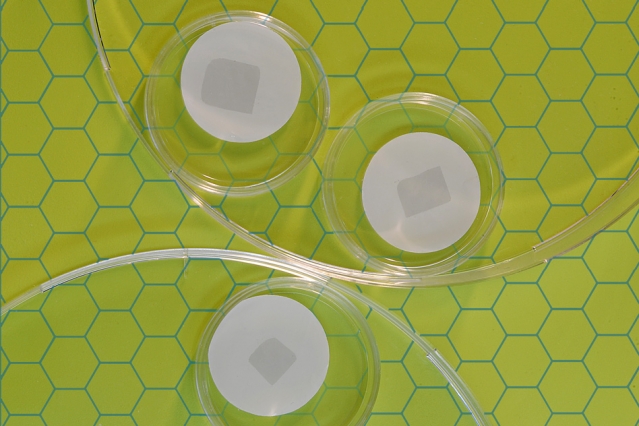
MIT researchers have developed a technique to fabricate large squares of graphemes that can filter out small molecules and salts. Image: Felice Frankel
Kidambi and his colleagues previously developed a technique to generate nanometer-sized pores in graphene, by first fabricating pristine graphene using conventional methods, then using oxygen plasma to etch away at the fully formed material to create pores.
Other groups have used focused beams of ions to methodically drill holes into graphene, but Kidambi says these techniques are difficult to integrate into any large-scale manufacturing process.
“Scalability of these processes are extremely limited,” Kidambi says.
“They would take way too much time, and in an industrially quick process, such pore-generating techniques would be challenging to do.”
So he looked for ways to make nanoporous graphene in a more direct fashion. As a PhD student at Cambridge University, Kidambi spent much of his time looking for ways to make pristine, defect-free graphene, for use in electronics. In that context, he was trying to minimize the defects in graphene that occurred during chemical vapor deposition (CVD) — a process by which researchers flow gas across a copper substrate within a furnace.
At high enough temperatures, of about 1,000 degrees Celsius, the gas eventually settles onto the substrate as high quality graphene.
“That was when the realization hit me: I just have to go back to my repository of processes and pick out those which give me defects, and try them in our CVD furnace,” Kidambi says.
As it turns out, the team found that by simply lowering the temperature of the furnace to between 850 and 900 degrees Celsius, they were able to directly produce nanometer-sized pores as the graphene was grown.
“When we tried this, it surprised us a little that it really works,” Kidambi says.
“This [temperature] condition really gave us the sizes we need to make graphene dialysis membranes.”
“This is one of several advances that will ultimately make graphene membranes practical for a range of applications,” Karnik adds.
“They may find use in biotechnological separations including in the preparation of drugs or molecular therapeutics, or perhaps in dialysis therapies.”
While the team is not entirely sure why a lower temperature creates nanoporous graphene, Kidambi suspects that it has something to do with how the gas in the reaction is deposited onto the substrate.
“The way graphene grows is, you inject a gas and the gas disassociates on the catalyst surface and forms carbon atom clusters which then form nuclei, or seeds,” Kidambi explains.
“So you have many small seeds that graphene can start growing from to form a continuous film. If you reduce the temperature, your threshold for nucleation is lower so you get many nuclei. And if you have too many nuclei, they can’t grow big enough, and they are more prone to defects. We don’t know exactly what the formation mechanism of these defects, or pores, is, but we see it every single time.”
The researchers were able to fabricate nanoporous sheets of graphene. But as the material is incredibly thin, and now pocked with holes, alone, it would likely come apart like paper-thin Swiss cheese if any solution of molecules were to flow across it.
So the team adapted a method to cast a thicker supporting layer of polymer on top of the graphene.
The supported graphene was now tough enough to withstand normal dialysis procedures. But even if target molecules were to pass through the graphene, they would be blocked by the polymer support.
The team needed a way to produce pores in the polymer that were significantly larger than those in graphene, to ensure that any small molecules passing through the ultrathin material would easily and quickly pass through the much thicker polymer, similar to a fish swimming through a port hole just its size, and then immediately passing through a much large tunnel.
The team ultimately found that by submersing the stack of copper, graphene, and polymer in a solution of water, and using conventional processes to etch away the copper layer, the same process naturally created large pores in the polymer support that were hundreds of times larger than the pores in graphene.
Combining their techniques, they were able to create sheets of nanoporous graphene, each measuring about 5 square centimeters.
“To the best of our knowledge, so far this is the largest atomically thin nanoporous membrane made by direct formation of pores,” Kidambi says.
Currently, the team has produced pores in graphene measuring approximately 2 to 3 nanometers wide, which they found was small enough to quickly filter salts such as potassium chloride (0.66 nanometers), and small molecules such as the amino acid L-Tryptophan (about 0.7 nanometers), food coloring Allura Red Dye (1 nanometer), and vitamin B-12 (1.5 nanometers) to varying degrees.
The material did not filter out slightly larger molecules, such as the egg protein lysozyme (4 nanometers). The team is now working to tailor the size of graphene pores to precisely filter molecules of various sizes.
“We now have to control these size defects and make tunable sized pores,” Kidambi says.
“Defects are not always bad, and if you can make the right defects, you can have many different applications for graphene.”
This research was supported, in part, by the U.S. Department of Energy.
Source: MIT