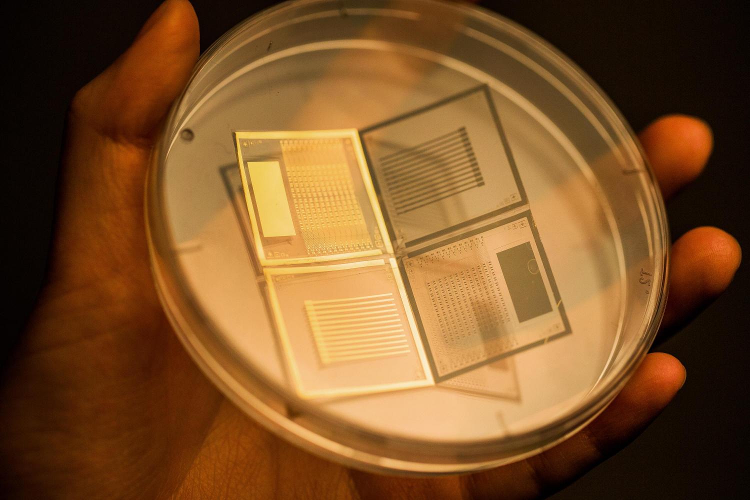
Transistor-type active-matrix 3D pressure sensors with air-dielectric layers. Image: UNIST
A recent study affiliated with UNIST has created a three-dimensional, tactile sensor that could detect wide pressure ranges from human body weight to a finger touch. This new sensor with transparent features is capable of generating an electrical signal based on the sensed touch actions, and also consumes far less electricity than conventional pressure sensors.
The breakthrough comes from research conducted by Professor Jang-Ung Park of Materials Science and Engineering and his research team at UNIST. In the study, the research team presented a novel method of fabricating a transistor-type active-matrix pressure sensor using foldable substrates and air-dielectric layers.
Today, most transistors are created with silicon channel and silicon oxide-based dielectrics. However, these transistors have been found to be either lacking transparency or inflexible, which may hinder their utility in fabricating highly-integrated pressure sensor arrays and transparent pressure sensors.
In this regard, Park’s team decided to use highly-conductive and transparent graphene transistors with air-dielectric layers. The sensor can detect different types of touch-including swiping and tapping.
“Using air as the dielectric layer in graphene field-effect transistors (FETs) can significantly improve transistor performance due to the clean interface between graphene channel and air,” says Park. “The thickness of the air-dielectric layers is determined by the applied pressure. With that technology, it would be possible to detect pressure changes far more effectively.”
A conventional touch panel, which may be included in a display device, reacts to the static electrical when pressure is applied to the monitor screen. With this method, the position on screen contacted by a finger, stylus, or other object can be easily detected using changes in pressure, but cannot provide the intensity of pressure.
The research team placed graphene channel, metal nanowire electrodes, as well as an elastic body capable of trapping air on one side of the foldable substrate. Then they covered the other side of the substrate, like a lid and kept the air. In this transistor, the force pressing the elastic body is transferred to the air-dielectric layer and alters its thickness. Such changes in the thickness of the air-dielectric layer is converted into an electrical signal and transmitted via metal nanowires and the graphene channel, expressing both the position and the intensity of the pressure.
This is regarded as a promising technology as it enables the successful implementation of active-matrix pressure sensors. Moreover, when compared with the passive-matrix type, it consumes less power and has a faster response time.
It is possible to send and receive signals only by flowing electricity to the place where pressure is generated. The change in the thickness of the air dielectric layer is converted into an electrical signal to represent the position and intensity of the pressure. In addition, since all the substrates, channels, and electrode materials used in this process are all transparent, they can also be manufactured with invisible pressure sensors.
“This sensor is capable of simultaneously measuring anything from lower pressure (less than 10 kPa), such as gentle tapping to high pressure (above 2 MPa), such as human body weight,” says Sangyoon Ji (Combined M.S./Ph.D. student of Materials Science and Engineering), the first co-author of the study. “It can be also applied to 3D touchscreen panels or smart running shoes that can analyze life patterns of people by measuring their weight distribution.”
“This study not only solves the limitations of conventional pressure sensors, but also suggests the possibility to apply them to various fields by combining pressure sensor with other electronic devices such as display,” says Park.
Source: UNIST