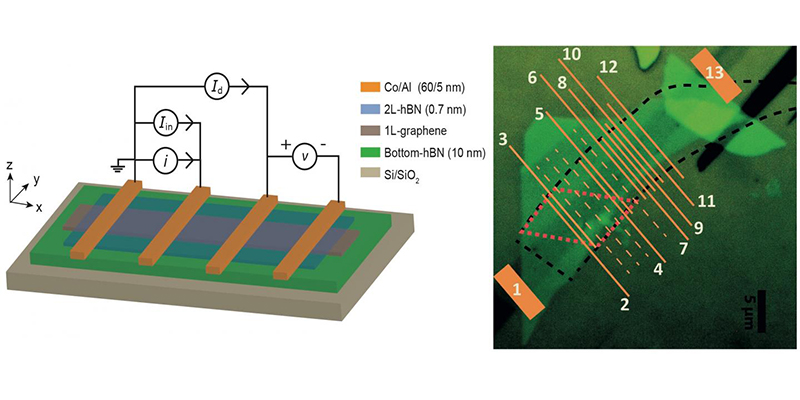
A layer-by-layer schematic alongside an optical microscopic picture of a graphene and boron nitride heterostructure device which shows unprecedented spin transport efficiency at room temperature. Credit: M. Gurram, S. Omar and B.J. van Wees, University of Groningen.
Graphene Flagship scientists based at the University of Groningen, The Netherlands, have created a device based on a bilayer of graphene and boron nitride which shows unprecedented spin transport efficiency at room temperature. Highlighting the potential of creating devices containing graphene and related materials, the spin signal measured here is so large that it can be used in real life applications such as spin based logic and transistors.
Published in Nature Communications, this research, led by Professor Bart van Wees, University of Groningen, The Netherlands, reports a graphene-based device in which electron spins can be injected and detected at room temperature with high efficiency. The key here is the interplay between the graphene and the boron nitride in the way that they conduct electron spins.
Spin can be thought of as the rotation of an electron around its own axis. It is a form of intrinsic angular momentum and can be detected as a magnetic field with one of two orientations: up and down. Electron spin is difficult to handle and often loses direction over time. To use electron spin in a device, spin polarisation is important – this is the ability to control the fraction of electrons with a spin up or down. ‘Spin polarization can be achieved by sending the electrons through a ferromagnetic material’, van Wees explains.
Professor van Wees and his team showed that they could greatly improve the efficiency of the injection and detection of spin electrons into graphene by using the insulator boron nitride in between the graphene layer and the ferromagnetic spin injector/detector electrodes.
“Graphene is a very good material for spin transport, but it does not allow one to manipulate the spins,” says van Wees “To inject spins into the graphene, one has to make them pass from a ferromagnet through a boron nitride insulator by quantum tunnelling. We found that using a two-atom layer of boron nitride resulted in a very strong spin polarization of up to 70 percent, ten times what we usually get.”
In the devices produced the polarization increased with voltage, challenging the current thinking that it is only the ferromagnetic that polarises spin. Instead it would seem that it is the quantum tunnelling that polarises the spin in his devices. The researchers also found a similar tenfold increase in spin detection in the same device. “So overall, the signal increased by a factor of 100.” said van Wees.
This creates many possibilities. “We can now inject spins into graphene and measure them easily after they travel some distance. One application would be as a detector for magnetic fields, which will affect the spin signal.” Another possibility would be to build a spin logic gate or a spin transistor. As the experiments with the new device were conducted at room temperature such applications are quite close. “However,” van Wees warns, “we used graphene which we obtained by exfoliation, using Scotch tape to peel monolayers off a piece of graphite. This is not suitable for large scale production.” Techniques to make high quality graphene on an industrial scale are a focus within the Graphene Flagship with the Work Package Production dedicated to this task.
Speaking about this research is Professor Vladimir Falko, Leader of Enabling Science and Materials Division of the Graphene Flagship: “Encapsulation of graphene in boron nitride and the use of heterostructures of these two materials for new devices, including tunnelling transistors, is a promising trend in graphene research that has previously delivered many interesting results. The reported observation takes graphene spintronics to the qualitatively new level.”
Spintronics is one of the work packages in the Graphene Flagship where Professor van Wees is the leader. It focuses on investigating room temperature graphene spintronic devices, joining together theoretical and experimental research and is seen as a long term investment for the Graphene Flagship. With so much progress being made on the individual elements that are needed to produce fully functional spintronic devices by the Graphene Flagship’s spintronics researchers, the next step is joining these together. The recently published work of Graphene Flagship Partner Professor Saroj Dash of Chalmers University, Sweden, showed the ability to control the amount of spin with a gate voltage – all at room temperature. Facilitating the collaboration on projects such as these is a central aim of the Graphene Flagship.
Professor Andrea Ferrari, Chair of the Management Panel and Science and Technology Officer of the Graphene Flagship added: “Spintronics has been one of the fundamental work packages since the start of the Flagship. It was always seen as a long term investment. It is exciting to see that so much progress has been made towards devices.”
Professor Stephan Roche, Spintronics Work Package Deputy Leader commented further: “This experimental breakthrough evidences that the Spintronics work package is acting as a pathfinder to bring all the potential of graphene and related materials to future practical applications in spintronics. It is however also clear that more efforts and investment are crucially needed to accelerate large scale integration of such type of realizations into the European fab environment for acquiring industrial leadership beyond the recognized European scientific excellence in this field.”
SOURCE: Graphene Flagship