Research & Development World

  • R&D World Home
  • Topics
    • Aerospace
    • Automotive
    • Biotech
    • Careers
    • Chemistry
    • Environment
    • Energy
    • Life Science
    • Material Science
    • R&D Management
    • Physics
  • Technology
    • 3D Printing
    • A.I./Robotics
    • Software
    • Battery Technology
    • Controlled Environments
      • Cleanrooms
      • Graphene
      • Lasers
      • Regulations/Standards
      • Sensors
    • Imaging
    • Nanotechnology
    • Scientific Computing
      • Big Data
      • HPC/Supercomputing
      • Informatics
      • Security
    • Semiconductors
  • R&D Market Pulse
  • R&D 100
    • Call for Nominations: The 2025 R&D 100 Awards
    • R&D 100 Awards Event
    • R&D 100 Submissions
    • Winner Archive
    • Explore the 2024 R&D 100 award winners and finalists
  • Resources
    • Research Reports
    • Digital Issues
    • Educational Assets
    • R&D Index
    • Subscribe
    • Video
    • Webinars
  • Global Funding Forecast
  • Top Labs
  • Advertise
  • SUBSCRIBE

3D Inks That Can Be Erased Selectively

By Karlsruher Institut Für Technologie (Kit) | August 15, 2018

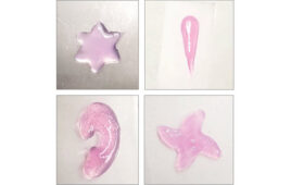
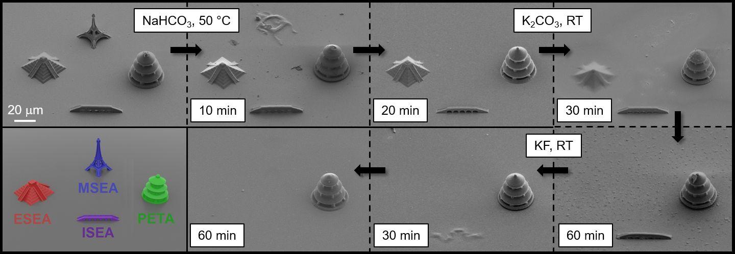
These are three-dimensional microstructures made of various cleavable photoresists. The scanning electron microscopies show the selective degradation of the structures (scaling 20 μm). Credit: Nature Communications

3D printing by direct laser writing enables production of micro-meter-sized structures for many applications, from biomedicine to microelectronics to optical metamaterials. Researchers of Karlsruhe Institute of Technology (KIT) have now developed 3D inks that can be erased selectively. This allows specific degradation and reassembly of highly precise structures on the micrometer and nanometer scales. The new photoresists are presented in the journal Nature Communications (DOI: 10.1038/s41467-018-05234-0).

3D printing is gaining importance, as it allows for the efficient manufacture of complex geometries. A very promising method is direct laser writing: a computer-controlled focused laser beam acts as a pen and produces the desired structure in a photoresist. In this way, three-dimensional structures with details in the sub-micrometer range can be produced. “The high resolution is very attractive for applications requiring very precise filigree structures, such as in biomedicine, microfluidics, microelectronics or for optical metamaterials,” say Professor Christopher Barner-Kowollik, Head of the Macromolecular Architectures Group of KIT’s Institute for Chemical Technology and Polymer Chemistry (ITCP) and of the Soft Matter Materials Group of Queensland University of Technology (QUT) in Brisbane, Australia, and Dr. Eva Blasco of the ITCP of KIT. Over a year ago, KIT researchers already succeeded in expanding the possibilities of direct laser writing: the working groups of Professor Martin Wegener at the Institute of Applied Physics (APH) and the Institute of Nanotechnology (INT) of KIT and of Professor Christopher Barner-Kowollik developed an erasable ink for 3D printing. Thanks to reversible binding, the building blocks of the ink can be separated again.

Now, the scientists from Karlsruhe and Brisbane have largely refined their development. As reported in the journal Nature Communications, they have developed several inks, in different colors so to speak, that can be erased independently of each other. This enables selective and sequential degradation and reassembly of the laser-written microstructures. In case of highly complex constructions, for instance, temporary supports can be produced and removed again later on. It may also be possible to add or remove parts to or from three-dimensional scaffolds for cell growth, the objective being to observe how the cells react to such changes. Moreover, the specifically erasable 3D inks allow for the exchange of damaged or worn parts in complex structures.

When producing the cleavable photoresists, the researchers were inspired by degradable biomaterials. The photoresists are based on silane compounds that can be cleaved easily. Silanes are silicon-hydrogen compounds. The scientists used specific atom substitution for preparing the photoresists. In this way, microstructures can be degraded specifically under mild conditions without structures with other material properties being damaged. This is the major advantage over formerly used erasable 3D inks. New photoresists also contain the monomer pentaerythritol triacrylate that significantly enhances writing without affecting cleavability.

Related Articles Read More >

Caltech team 3D-prints drug depots deep inside living tissue
What could make MXene a key to ultra-precise, additive-free 3D microprinting?
Industry 4.0 Modern Factory: Facility Operator Controls Workshop Production Line, Uses Computer with Screens Showing Complex UI of Machine Operation Processes, Controllers, Machinery Blueprints
Building the thinking factory: An additive exec on AI, automation, and the skills crisis
Red Bull and Mercedes F1 cars 3D illustration, 30 Aug, 2022, Texas, EUA
6 technologies pushing Formula 1’s engineering frontier
rd newsletter
EXPAND YOUR KNOWLEDGE AND STAY CONNECTED
Get the latest info on technologies, trends, and strategies in Research & Development.
RD 25 Power Index

R&D World Digital Issues

Fall 2024 issue

Browse the most current issue of R&D World and back issues in an easy to use high quality format. Clip, share and download with the leading R&D magazine today.

Research & Development World
  • Subscribe to R&D World Magazine
  • Enews Sign Up
  • Contact Us
  • About Us
  • Drug Discovery & Development
  • Pharmaceutical Processing
  • Global Funding Forecast

Copyright © 2025 WTWH Media LLC. All Rights Reserved. The material on this site may not be reproduced, distributed, transmitted, cached or otherwise used, except with the prior written permission of WTWH Media
Privacy Policy | Advertising | About Us

Search R&D World

  • R&D World Home
  • Topics
    • Aerospace
    • Automotive
    • Biotech
    • Careers
    • Chemistry
    • Environment
    • Energy
    • Life Science
    • Material Science
    • R&D Management
    • Physics
  • Technology
    • 3D Printing
    • A.I./Robotics
    • Software
    • Battery Technology
    • Controlled Environments
      • Cleanrooms
      • Graphene
      • Lasers
      • Regulations/Standards
      • Sensors
    • Imaging
    • Nanotechnology
    • Scientific Computing
      • Big Data
      • HPC/Supercomputing
      • Informatics
      • Security
    • Semiconductors
  • R&D Market Pulse
  • R&D 100
    • Call for Nominations: The 2025 R&D 100 Awards
    • R&D 100 Awards Event
    • R&D 100 Submissions
    • Winner Archive
    • Explore the 2024 R&D 100 award winners and finalists
  • Resources
    • Research Reports
    • Digital Issues
    • Educational Assets
    • R&D Index
    • Subscribe
    • Video
    • Webinars
  • Global Funding Forecast
  • Top Labs
  • Advertise
  • SUBSCRIBE