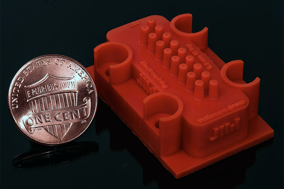
A 3-D-printed manufacturing device can extrude fibers that are only 75 nanometers in diameter, or one-thousandth the width of a human hair. Image: Luis Fernando Velásquez-García
Meshes made from fibers with nanometer-scale diameters have a wide range of potential applications, including tissue engineering, water filtration, solar cells, and even body armor. But their commercialization has been hampered by inefficient manufacturing techniques.
In the latest issue of the journal Nanotechnology, MIT researchers describe a new device for producing nanofiber meshes, which matches the production rate and power efficiency of its best-performing predecessor — but significantly reduces variation in the fibers’ diameters, an important consideration in most applications.
But whereas the predecessor device, from the same MIT group, was etched into silicon through a complex process that required an airlocked “clean room,” the new device was built using a $3,500 commercial 3-D printer. The work thus points toward nanofiber manufacture that is not only more reliable but also much cheaper.
The new device consists of an array of small nozzles through which a fluid containing particles of a polymer are pumped. As such, it is what’s known as a microfluidic device.
“My personal opinion is that in the next few years, nobody is going to be doing microfluidics in the clean room,” says Luis Fernando Velásquez-García, a principal research scientist in MIT’s Microsystems Technology Laboratories and senior author on the new paper. “There’s no reason to do so. 3-D printing is a technology that can do it so much better — with better choice of materials, with the possibility to really make the structure that you would like to make. When you go to the clean room, many times you sacrifice the geometry you want to make. And the second problem is that it is incredibly expensive.”
Velásquez-García is joined on the paper by two postdocs in his group, Erika García-López and Daniel Olvera-Trejo. Both received their PhDs from Tecnológico de Monterrey in Mexico and worked with Velásquez-García through MIT and Tecnológico de Monterrey’s nanotech research partnership.
Hollowed out
Nanofibers are useful for any application that benefits from a high ratio of surface area to volume — such as solar cells, which try to maximize exposure to sunlight, or fuel cell electrodes, which catalyze reactions at their surfaces. Nanofibers can also yield materials that are permeable only at very small scales, such as water filters, or that are remarkably tough for their weight, such as body armor.
Most such applications depend on fibers with regular diameters. “The performance of the fibers strongly depends on their diameter,” Velásquez-García says. “If you have a significant spread, what that really means is that only a few percent are really working. Example: You have a filter, and the filter has pores between 50 nanometers and 1 micron. That’s really a 1-micron filter.”
Because the group’s earlier device was etched in silicon, it was “externally fed,” meaning that an electric field drew a polymer solution up the sides of the individual emitters. The fluid flow was regulated by rectangular columns etched into the sides of the emitters, but it was still erratic enough to yield fibers of irregular diameter.
The new emitters, by contrast, are “internally fed”: They have holes bored through them, and hydraulic pressure pushes fluid into the bores until they’re filled. Only then does an electric field draw the fluid out into tiny fibers.
Beneath the emitters, the channels that feed the bores are wrapped into coils, and they gradually taper along their length. That taper is key to regulating the diameter of the nanofibers, and it would be virtually impossible to achieve with clean-room microfabrication techniques. “Microfabrication is really meant to make straight cuts,” Velásquez-García says.
Fast iteration
In the new device, the nozzles are arranged into two rows, which are slightly offset from each other. That’s because the device was engineered to demonstrate aligned nanofibers — nanofibers that preserve their relative position as they’re collected by a rotating drum. Aligned nanofibers are particularly useful in some applications, such as tissue scaffolding. For applications in which unaligned fibers are adequate, the nozzles could be arranged in a grid, increasing output rate.
Besides cost and design flexibility, Velásquez-García says, another advantage of 3-D printing is the ability to rapidly test and revise designs. With his group’s microfabricated devices, he says, it typically takes two years to go from theoretical modeling to a published paper, and in the interim, he and his colleagues might be able to test two or three variations on their basic design. With the new device, he says, the process took closer to a year, and they were able to test 70 iterations of the design.
“A way to deterministically engineer the position and size of electrospun fibers allows you to start to think about being able to control mechanical properties of materials that are made from these fibers. It allows you to think about preferential cell growth along particular directions in the fibers — lots of good potential opportunities there,” says Mark Allen, the Alfred Fitler Moore Professor at the University of Pennsylvania, with joint appointments in electrical and systems engineering and mechanical engineering and applied mechanics. “I anticipate that somebody’s going to take this technology and use it in very creative ways. If you have the need for this type of deterministically engineered fiber network, I think it’s a very elegant way to achieve that goal.”