Research & Development World

  • R&D World Home
  • Topics
    • Aerospace
    • Automotive
    • Biotech
    • Careers
    • Chemistry
    • Environment
    • Energy
    • Life Science
    • Material Science
    • R&D Management
    • Physics
  • Technology
    • 3D Printing
    • A.I./Robotics
    • Software
    • Battery Technology
    • Controlled Environments
      • Cleanrooms
      • Graphene
      • Lasers
      • Regulations/Standards
      • Sensors
    • Imaging
    • Nanotechnology
    • Scientific Computing
      • Big Data
      • HPC/Supercomputing
      • Informatics
      • Security
    • Semiconductors
  • R&D Market Pulse
  • R&D 100
    • 2025 R&D 100 Award Winners
    • 2025 Professional Award Winners
    • 2025 Special Recognition Winners
    • R&D 100 Awards Event
    • R&D 100 Submissions
    • Winner Archive
  • Resources
    • Research Reports
    • Digital Issues
    • Educational Assets
    • Subscribe
    • Video
    • Webinars
    • Content submission guidelines for R&D World
  • Global Funding Forecast
  • Top Labs
  • Advertise
  • SUBSCRIBE

3D-Printing at the Nanoscale

By Oak Ridge National Laboratory | December 5, 2016

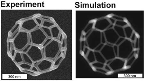
A 32-face 3D truncated icosahedron mesh was created to test a simulation’s ability to guide precise construction of complex geometries. Scanning electron microscopy of the product (left) showed excellent agreement with the nanoscale structure that the simulation predicted (right). Image: © American Chemical Society

Realization of “3D printing” material assembly on the micron or even nanometer scale has posed significant challenges to researchers. Now, scientists have developed a specialized computer simulation that guides an electron beam to create custom 3D structures (ACS Nano, “Simulation guided 3D nanomanufacturing via focused electron beam induced deposition”).

The beam induces a precursor material to deposit in a way that forms complex shapes. This nanoscale 3D printing creates freestanding structures so tiny that bacteria dwarf them.

The new approach, simulation-guided material deposition at the nanoscale, offers a path to synthesize materials with superior mechanical and optical properties. This design approach replaces trial-and-error in nanomanufacturing for materials and structures with superior mechanical and optical properties.

Precision control of nanometer scale 3D fabrication has been a longstanding research goal. Now, researchers have developed a 3D simulation that guides focused electron beam induced deposition (FEBiD) of precursor molecules on a surface and accurately predicts the complex geometries of deposited shapes over the length scale from nanometers to micrometers.

The simulation predicts gas-solid interactions where the electron beam strikes a surface. While FEBiD can direct-write freestanding 3D nanostructures, improved understanding of the dynamic interplay of the scanning electron beam and adsorbed precursor molecules is critical for advancing additive manufacturing of optoelectronics, metamaterials, and more.

The simulations consist of (1) a Monte Carlo simulation to calculate the electron–solid interaction and (2) a continuum simulation to calculate surface adsorption, desorption, diffusion, and deposition of precursor molecules.

The merged simulation can guide the electron beam to produce complex lattices and meshes sized between 10 nanometers and 1 micron.

Source: Oak Ridge National Laboratory  

Related Articles Read More >

R&D 100 winner LLNL achieves 1,000x speed boost in 3D nanofabrication
Caltech team 3D-prints drug depots deep inside living tissue
What could make MXene a key to ultra-precise, additive-free 3D microprinting?
Industry 4.0 Modern Factory: Facility Operator Controls Workshop Production Line, Uses Computer with Screens Showing Complex UI of Machine Operation Processes, Controllers, Machinery Blueprints
Building the thinking factory: An additive exec on AI, automation, and the skills crisis
rd newsletter
EXPAND YOUR KNOWLEDGE AND STAY CONNECTED
Get the latest info on technologies, trends, and strategies in Research & Development.

R&D World Digital Issues

Fall 2025 issue

Browse the most current issue of R&D World and back issues in an easy to use high quality format. Clip, share and download with the leading R&D magazine today.

R&D 100 Awards
Research & Development World
  • Subscribe to R&D World Magazine
  • Sign up for R&D World’s newsletter
  • Contact Us
  • About Us
  • Drug Discovery & Development
  • Pharmaceutical Processing
  • Global Funding Forecast

Copyright © 2026 WTWH Media LLC. All Rights Reserved. The material on this site may not be reproduced, distributed, transmitted, cached or otherwise used, except with the prior written permission of WTWH Media
Privacy Policy | Advertising | About Us

Search R&D World

  • R&D World Home
  • Topics
    • Aerospace
    • Automotive
    • Biotech
    • Careers
    • Chemistry
    • Environment
    • Energy
    • Life Science
    • Material Science
    • R&D Management
    • Physics
  • Technology
    • 3D Printing
    • A.I./Robotics
    • Software
    • Battery Technology
    • Controlled Environments
      • Cleanrooms
      • Graphene
      • Lasers
      • Regulations/Standards
      • Sensors
    • Imaging
    • Nanotechnology
    • Scientific Computing
      • Big Data
      • HPC/Supercomputing
      • Informatics
      • Security
    • Semiconductors
  • R&D Market Pulse
  • R&D 100
    • 2025 R&D 100 Award Winners
    • 2025 Professional Award Winners
    • 2025 Special Recognition Winners
    • R&D 100 Awards Event
    • R&D 100 Submissions
    • Winner Archive
  • Resources
    • Research Reports
    • Digital Issues
    • Educational Assets
    • Subscribe
    • Video
    • Webinars
    • Content submission guidelines for R&D World
  • Global Funding Forecast
  • Top Labs
  • Advertise
  • SUBSCRIBE