Research & Development World

  • R&D World Home
  • Topics
    • Aerospace
    • Automotive
    • Biotech
    • Careers
    • Chemistry
    • Environment
    • Energy
    • Life Science
    • Material Science
    • R&D Management
    • Physics
  • Technology
    • 3D Printing
    • A.I./Robotics
    • Software
    • Battery Technology
    • Controlled Environments
      • Cleanrooms
      • Graphene
      • Lasers
      • Regulations/Standards
      • Sensors
    • Imaging
    • Nanotechnology
    • Scientific Computing
      • Big Data
      • HPC/Supercomputing
      • Informatics
      • Security
    • Semiconductors
  • R&D Market Pulse
  • R&D 100
    • 2025 R&D 100 Award Winners
    • 2025 Professional Award Winners
    • 2025 Special Recognition Winners
    • R&D 100 Awards Event
    • R&D 100 Submissions
    • Winner Archive
  • Resources
    • Research Reports
    • Digital Issues
    • Educational Assets
    • R&D Index
    • Subscribe
    • Video
    • Webinars
    • Content submission guidelines for R&D World
  • Global Funding Forecast
  • Top Labs
  • Advertise
  • SUBSCRIBE

A New Way to Alter Boron Nitride

By University of Illinois at Chicago | September 26, 2018

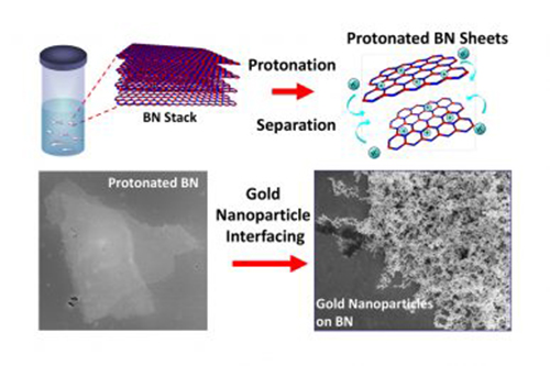
Treatment with a superacid causes boron nitride layers to separate and become positively charged, allowing for interface with other nanomaterials, like gold. Imaget: Berry, et al.

Researchers at the University of Illinois at Chicago have discovered a route to alter boron nitride, a layered 2D material, so that it can bind to other materials, like those found in electronics, biosensors, and airplanes, for example.

Being able to better-incorporate boron nitride into these components could help dramatically improve their performance.

The scientific community has long been interested in boron nitride because of its unique properties —it is strong, ultrathin, transparent, insulating, lightweight and thermally conductive — which, in theory, makes it a perfect material for use by engineers in a wide variety of applications.

However, boron nitride’s natural resistance to chemicals and lack of surface-level molecular binding sites have made it difficult for the material to interface with other materials used in these applications.

UIC’s Vikas Berry and his colleagues are the first to report that treatment with a superacid causes boron nitride layers to separate into atomically thick sheets, while creating binding sites on the surface of these sheets that provide opportunities to interface with nanoparticles, molecules and other 2D nanomaterials, like graphene. This includes nanotechnologies that use boron nitride to insulate nano-circuits.

Their findings are published in ACS Nano, a journal of the American Chemical Society.

“Boron nitride is like a stack of highly sticky papers in a ream, and by treating this ream with chlorosulfonic acid, we introduced positive charges on the boron nitride layers that caused the sheets to repel each other and separate,” says Berry, associate professor and head of chemical engineering at the UIC College of Engineering and corresponding author on the paper.

Berry says that “like magnets of the same polarity,” these positively charged boron nitride sheets repel one another.

“We showed that the positive charges on the surfaces of the separated boron nitride sheets make it more chemically active,” Berry says.

“The protonation — the addition of positive charges to atoms — of internal and edge nitrogen atoms creates a scaffold to which other materials can bind.”

Berry says that the opportunities for boron nitride to improve composite materials in next-generation applications are vast.

“Boron and nitrogen are on the left and the right of carbon on the periodic table and therefore, boron-nitride is isostructural and isoelectronic to carbon-based graphene, which is considered a ‘wonder material,’” Berry says.

This means these two materials are similar in their atomic crystal structure (isostructural) and their overall electron density (isoelectric), he says.

“We can potentially use this material in all kinds of electronics, like optoelectronic and piezoelectric devices, and in many other applications, from solar-cell passivation layers, which function as filters to absorb only certain types of light, to medical diagnostic devices,” Berry says.

Co-authors on the study are Sanjay Behura of UIC; Kabeer Jasuja of the Indian Institute of Technology; and Kayum Ayinde, Christina Wilson, Myles Ikenberry, Keith Hon, and David Moore of Kansas State University.

Source: University of Illinois at Chicago

Related Articles Read More >

R&D 100 winner flags even unknown fentanyl analogs
New nanopore sensor paves the way for fast, accurate, low-cost DNA sequencing
IoT
Sensor data, reimagined: When 90% less data can fuel 100x gains in efficiency in AI projects
Sandia Labs joins with other institutions to tackle AI energy challenges with microelectronics research
rd newsletter
EXPAND YOUR KNOWLEDGE AND STAY CONNECTED
Get the latest info on technologies, trends, and strategies in Research & Development.
RD 25 Power Index

R&D World Digital Issues

Fall 2025 issue

Browse the most current issue of R&D World and back issues in an easy to use high quality format. Clip, share and download with the leading R&D magazine today.

R&D 100 Awards
Research & Development World
  • Subscribe to R&D World Magazine
  • Sign up for R&D World’s newsletter
  • Contact Us
  • About Us
  • Drug Discovery & Development
  • Pharmaceutical Processing
  • Global Funding Forecast

Copyright © 2026 WTWH Media LLC. All Rights Reserved. The material on this site may not be reproduced, distributed, transmitted, cached or otherwise used, except with the prior written permission of WTWH Media
Privacy Policy | Advertising | About Us

Search R&D World

  • R&D World Home
  • Topics
    • Aerospace
    • Automotive
    • Biotech
    • Careers
    • Chemistry
    • Environment
    • Energy
    • Life Science
    • Material Science
    • R&D Management
    • Physics
  • Technology
    • 3D Printing
    • A.I./Robotics
    • Software
    • Battery Technology
    • Controlled Environments
      • Cleanrooms
      • Graphene
      • Lasers
      • Regulations/Standards
      • Sensors
    • Imaging
    • Nanotechnology
    • Scientific Computing
      • Big Data
      • HPC/Supercomputing
      • Informatics
      • Security
    • Semiconductors
  • R&D Market Pulse
  • R&D 100
    • 2025 R&D 100 Award Winners
    • 2025 Professional Award Winners
    • 2025 Special Recognition Winners
    • R&D 100 Awards Event
    • R&D 100 Submissions
    • Winner Archive
  • Resources
    • Research Reports
    • Digital Issues
    • Educational Assets
    • R&D Index
    • Subscribe
    • Video
    • Webinars
    • Content submission guidelines for R&D World
  • Global Funding Forecast
  • Top Labs
  • Advertise
  • SUBSCRIBE