Engineers Create Atomically Thin Superlattice Materials With Precision
Control is a constant challenge for materials scientists, who are always seeking the perfect material — and the perfect way of treating it — to induce exactly the right electronic or optical activity required for a given application. One key challenge to modulating activity in a semiconductor is controlling its band gap. When a material…
Bringing Deep Learning to Big Screen Animation
X-Ray Eyes in The Sky: Drones and Wifi For 3D Through-Wall Imaging
A Tiny Machine: Engineers Design an Infinitesimal Computing Device
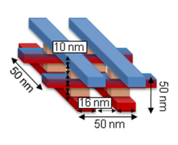
In 1959 renowned physicist Richard Feynman, in his talk “Plenty of Room at the Bottom,” spoke of a future in which tiny machines could perform huge feats. Like many forward-looking concepts, his molecule and atom-sized world remained for years in the realm of science fiction. And then, scientists and other creative thinkers began to realize…
Non-Toxic, High-Quality Surface Treatment for Organic Field-Effect Transistors
In a development beneficial for both industry and environment, UC Santa Barbara researchers have created a high-quality coating for organic electronics that promises to decrease processing time as well as energy requirements. “It’s faster, and it’s nontoxic,” said Kollbe Ahn, a research faculty member at UCSB’s Marine Science Institute and corresponding author of a paper…


