Research & Development World

  • R&D World Home
  • Topics
    • Aerospace
    • Automotive
    • Biotech
    • Careers
    • Chemistry
    • Environment
    • Energy
    • Life Science
    • Material Science
    • R&D Management
    • Physics
  • Technology
    • 3D Printing
    • A.I./Robotics
    • Software
    • Battery Technology
    • Controlled Environments
      • Cleanrooms
      • Graphene
      • Lasers
      • Regulations/Standards
      • Sensors
    • Imaging
    • Nanotechnology
    • Scientific Computing
      • Big Data
      • HPC/Supercomputing
      • Informatics
      • Security
    • Semiconductors
  • R&D Market Pulse
  • R&D 100
    • 2025 R&D 100 Award Winners
    • 2025 Professional Award Winners
    • 2025 Special Recognition Winners
    • R&D 100 Awards Event
    • R&D 100 Submissions
    • Winner Archive
  • Resources
    • Research Reports
    • Digital Issues
    • Educational Assets
    • Subscribe
    • Video
    • Webinars
    • PharmSci360
    • Content submission guidelines for R&D World
  • Global Funding Forecast
  • Top Labs
  • Advertise
  • SUBSCRIBE

Faster Nano Level Imaging Now Available

By Taylor McNeil, Tufts University | September 27, 2017

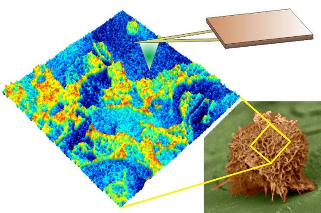
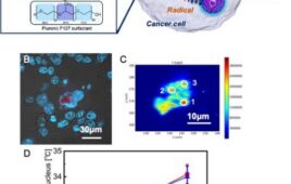
“This imaging mode will help develop new materials and processes,” said Igor Sokolov. Here, a cell surface showing the height of the pericellular layer around a cancer cell. Image: Maxim Dokukin and Igor Sokolov

Tufts University researchers have discovered a new, faster way to image materials at the nano level, an advance that could speed the detection of cancer and assist in the development of new high-tech materials.

The new method was discovered by Igor Sokolov, a professor of mechanical engineering, and Maxim Dokukin, a postdoctoral scholar in Sokolov’s lab. It extends the capacity of atomic force microscopy (AFM), a technology available since 1989 that allows imaging of samples down to the sub-nanometer level.

“This imaging mode will enable further scientific and technological understanding and help develop new materials and processes,” Sokolov says. “Better detection of cancer cells is what we have on the horizon at our lab. But it will also be most impactful in the area of nanocomposites and new multiphase polymers such as organic-inorganic biocomposites, in which the structure of materials down to the nanoscale is of critical importance.”

The Tufts researchers discovered a way to use new channels of information that had been traditionally discarded as noise in existing commercial AFM imaging methods. What they call the “ringing method” allows “more robust and novel information about the surface of biologically relevant materials, cells, and polymers,” the researchers wrote. When applied to soft materials, in particular cells, imaging can be done up to 20 times faster than conventional AFM methods.

That speed might make the technology useful in clinical settings, when trying to identify potentially cancerous cells, though biological applications for the time being will mostly be in the research arena, Sokolov says.

The researchers described the discovery in a paper last week in Scientific Reports, an open-access journal put out by the group that produces the journal Nature. Tufts earlier this year received a patent for the invention, and has already licensed its use to Nanoscience Solutions Inc., which is selling an AFM “ring method” add-on using this technology, says Sokolov.

“AFM is one of the major tools that has facilitated development of nanotechnology,” says Sokolov, who is also an adjunct professor in the Department of Biomedical Engineering and the Department of Physics. The new AFM imaging mode, he says, “will extend the capacity of this microscopy to quantify new characteristics of materials at a previously inaccessible scale.”

Source: Tufts University
Related Articles Read More >

Researchers developed quantum nanosensors that can measure the temperature of a single cell
Overcoming the 100-nanometer barrier: New microbottle resonators scale up optical trapping
R&D 100 winner LLNL achieves 1,000x speed boost in 3D nanofabrication
CEA-Leti achieves 400°C CMOS fabrication milestone for 3D chip stacking
rd newsletter
EXPAND YOUR KNOWLEDGE AND STAY CONNECTED
Get the latest info on technologies, trends, and strategies in Research & Development.

R&D World Digital Issues

Fall 2025 issue

Browse the most current issue of R&D World and back issues in an easy to use high quality format. Clip, share and download with the leading R&D magazine today.

R&D 100 Awards
Research & Development World
  • Subscribe to R&D World Magazine
  • Sign up for R&D World’s newsletter
  • Contact Us
  • About Us
  • Drug Discovery & Development
  • Pharmaceutical Processing
  • Global Funding Forecast

Copyright © 2026 Arrowfly LLC. All Rights Reserved. The material on this site may not be reproduced, distributed, transmitted, cached or otherwise used, except with the prior written permission of Arrowfly
Privacy Policy | Advertising | About Us

Search R&D World

  • R&D World Home
  • Topics
    • Aerospace
    • Automotive
    • Biotech
    • Careers
    • Chemistry
    • Environment
    • Energy
    • Life Science
    • Material Science
    • R&D Management
    • Physics
  • Technology
    • 3D Printing
    • A.I./Robotics
    • Software
    • Battery Technology
    • Controlled Environments
      • Cleanrooms
      • Graphene
      • Lasers
      • Regulations/Standards
      • Sensors
    • Imaging
    • Nanotechnology
    • Scientific Computing
      • Big Data
      • HPC/Supercomputing
      • Informatics
      • Security
    • Semiconductors
  • R&D Market Pulse
  • R&D 100
    • 2025 R&D 100 Award Winners
    • 2025 Professional Award Winners
    • 2025 Special Recognition Winners
    • R&D 100 Awards Event
    • R&D 100 Submissions
    • Winner Archive
  • Resources
    • Research Reports
    • Digital Issues
    • Educational Assets
    • Subscribe
    • Video
    • Webinars
    • PharmSci360
    • Content submission guidelines for R&D World
  • Global Funding Forecast
  • Top Labs
  • Advertise
  • SUBSCRIBE