
Research & Development World

  • R&D World Home
  • Topics
    • Aerospace
    • Automotive
    • Biotech
    • Careers
    • Chemistry
    • Environment
    • Energy
    • Life Science
    • Material Science
    • R&D Management
    • Physics
  • Technology
    • 3D Printing
    • A.I./Robotics
    • Software
    • Battery Technology
    • Controlled Environments
      • Cleanrooms
      • Graphene
      • Lasers
      • Regulations/Standards
      • Sensors
    • Imaging
    • Nanotechnology
    • Scientific Computing
      • Big Data
      • HPC/Supercomputing
      • Informatics
      • Security
    • Semiconductors
  • R&D Market Pulse
  • R&D 100
    • 2025 R&D 100 Award Winners
    • 2025 Professional Award Winners
    • 2025 Special Recognition Winners
    • R&D 100 Awards Event
    • R&D 100 Submissions
    • Winner Archive
  • Resources
    • Research Reports
    • Digital Issues
    • Educational Assets
    • Subscribe
    • Video
    • Webinars
    • PharmSci360
    • Content submission guidelines for R&D World
  • Global Funding Forecast
  • Top Labs
  • Advertise
  • SUBSCRIBE

Flatter Materials Have Fewer Imperfections, Which Makes for Better Solar Cells and Light Sensors

By King Abdullah University of Science & Technology | August 14, 2017

Improving the efficiency of materials will help to further advancements in designing and optimizing perovskite solar cells. (Credit: KAUST)

Improving the efficiency of solar cells requires materials free from impurities and structural defects. Scientists across many disciplines at KAUST have shown that 2-D organic-inorganic hybrid materials feature far fewer defects than thicker 3-D versions.

Modern-day electronics rely on technologies that can develop almost perfect crystals of silicon; flawless to the atomic level. This is crucial because defects and impurities scatter electrons as they flow, which adversely affects the material’s electronic properties.

But hybrid perovskites, an exciting class of electronic material, cannot be constructed using the epitaxial or layer methods developed for silicon. Instead, they are produced using solution-based processes. While this makes them cheaper than silicon, it also makes purity much harder to achieve as defect population and species are sensitive to the processing conditions.

Osman Bakr from the KAUST Solar Center together with colleagues from multiple divisions across KAUST and the University of Toronto, demonstrate that two-dimensional layers of perovskite material can achieve levels of purity much higher than is possible than in their 3-D counterpart. “Two-dimensional hybrid perovskites are a subgroup of the big hybrid perovskite family,” explains Wei Peng, lead author and doctoral degree recipient from Bakr’s lab. “They can be derived by inserting large organic cations in three-dimensional perovskite structures.”

Hybrid perovskites are made up of lead and halide (such as iodine) atoms and an organic component. This class of materials in solar cells has already shown ground-breaking potential for energy conversion efficiency while having low production costs and the possibility for being integrated in flexible devices. This combination of qualities makes hybrid perovskites an exciting material for optoelectronic applications.

Peng, Bakr and coworkers created a 2-D material made of periodic layers of hybrid perovskites with an organic component of either phenethylammonium or methylammonium. Using a solution-based fabrication method, the layers were placed on a gold electrode so the team could measure the electrical conductivity.

Their measurements indicate that the 2-D materials contained three orders of magnitude fewer defects than bulk hybrid perovskites. The team proposes that this reduction is because the large organic cations in the phenethylammonium suppress defect formation during crystallization.

Next, the team demonstrated the potential for their materials for optoelectronic applications by constructing photoconductors with high light detectivity. These results bode well for further advancements in designing and optimizing perovskite solar cells. “A future in-depth study on how the defect formation is suppressed will help our understanding and benefit device performance-targeted materials engineering,” says Peng.

Related Articles Read More >

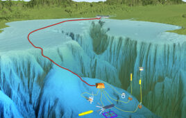
MBARI's Monterey Accelerated Research System (MARS) connects seafloor instruments to shore through a roughly 51-kilometer power and fiber-optic cable (red line) ending at a node about 891 meters down. The Geo-Sense system described in the new paper takes the opposite approach: a portable, battery-powered cable that records locally with no link to shore. Researchers used MARS's own fiber data to cross-check Geo-Sense's earthquake detections. Credit: MBARI
How lightweight AI startup Lightscline helped turn one to two years of seafloor data analysis into a two-month sprint
UC Riverside’s $5 fake drug detector uses toy robot sensors to catch counterfeit medications
R&D 100 winner flags even unknown fentanyl analogs
New nanopore sensor paves the way for fast, accurate, low-cost DNA sequencing
rd newsletter
EXPAND YOUR KNOWLEDGE AND STAY CONNECTED
Get the latest info on technologies, trends, and strategies in Research & Development.

R&D World Digital Issues

Fall 2025 issue

Browse the most current issue of R&D World and back issues in an easy to use high quality format. Clip, share and download with the leading R&D magazine today.

R&D 100 Awards
Research & Development World
  • Subscribe to R&D World Magazine
  • Sign up for R&D World’s newsletter
  • Contact Us
  • About Us
  • Drug Discovery & Development
  • Pharmaceutical Processing
  • Global Funding Forecast

Copyright © 2026 Arrowfly LLC. All Rights Reserved. The material on this site may not be reproduced, distributed, transmitted, cached or otherwise used, except with the prior written permission of Arrowfly
Privacy Policy | Advertising | About Us

Search R&D World

  • R&D World Home
  • Topics
    • Aerospace
    • Automotive
    • Biotech
    • Careers
    • Chemistry
    • Environment
    • Energy
    • Life Science
    • Material Science
    • R&D Management
    • Physics
  • Technology
    • 3D Printing
    • A.I./Robotics
    • Software
    • Battery Technology
    • Controlled Environments
      • Cleanrooms
      • Graphene
      • Lasers
      • Regulations/Standards
      • Sensors
    • Imaging
    • Nanotechnology
    • Scientific Computing
      • Big Data
      • HPC/Supercomputing
      • Informatics
      • Security
    • Semiconductors
  • R&D Market Pulse
  • R&D 100
    • 2025 R&D 100 Award Winners
    • 2025 Professional Award Winners
    • 2025 Special Recognition Winners
    • R&D 100 Awards Event
    • R&D 100 Submissions
    • Winner Archive
  • Resources
    • Research Reports
    • Digital Issues
    • Educational Assets
    • Subscribe
    • Video
    • Webinars
    • PharmSci360
    • Content submission guidelines for R&D World
  • Global Funding Forecast
  • Top Labs
  • Advertise
  • SUBSCRIBE