National University of Singapore researchers have discovered a simple and effective method to produce a large area pseudo-magnetic field (PMF) on graphene, and demonstrated how it can be tuned with desired spatial distribution and intensity for data storage and logic applications (“Tailoring sample-wide pseudo-magnetic fields on a graphene-black phosphorus heterostructure”).
The field of electronics focuses on how to control and exploit the properties of electrons. To study or modify the properties of these electrons at the quantum regime, a magnetic field has to be applied.
Another way of achieving this effect is to mechanically create a special type of strain in graphene, where the electrons behave as if they are under the influence of an externally applied magnetic field. In this case, no magnetic field is physically applied and this is explained by the presence of strain-induced PMF.
Electrons have additional degrees of freedom (independent parameter describing the electronic state) other than its charge. These are known as the spins and valley degree of freedom. Strain-induced PMFs in graphene have been explored as a promising approach to pull apart the valleys in graphene and make their energies non-equivalent, producing intriguing physics such as valley-polarized current. Many researchers have been attracted by the enormous PMFs (up to 300 teslas) observed in non-planar, strained graphene nanostructures such as graphene nanobubbles.
However, these are distributed randomly and they are not feasible for practical implementation. Although theory predicts that strains with triangular symmetry are able to create PMF in materials, there is currently no known experimental technique which can create the specific strain texture to generate a uniform PMF with the desired spatial distribution and intensity.
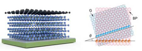
(Left) The lattice mismatch between the monolayer graphene (black) on multilayer black phosphorous (blue) generates PMF on the graphene layer. (Right) The spatial distribution and intensity of the PMF can be tailored by changing the rotation angle between the graphene and black phosphorous. Image: NUS
A team led by Professor Loh Kian Ping from the Department of Chemistry and Centre for Advanced 2D Materials has discovered a way to generate PMFs on graphene by overlaying graphene on black phosphorous (BP) to form a graphene-on-BP heterostructure. The research team also includes surface chemist Professor Lu Jiong and theoretician Professor Adam Shaffique from NUS. The large lattice mismatch and shear strain imposed by the lattices on each other give rise to PMFs on graphene, which can be measured directly using scanning tunneling microscopy.
In addition, they discovered a way to tailor the intensity and spatial distribution of the PMFs on graphene by changing the rotation angle between the crystallographic directions of the graphene and the BP. When an external magnetic field is applied in the presence of the PMF, they are able to create two types of non-equivalent currents, known as the valley-polarized current in electrical transport measurements.
Loh says, “Controlling PMFs at the nanoscale allows the following extreme physics to be tested: first, the PMF fields can serve as energy barriers to efficiently confine currents into a one-dimensional channel. In addition, valley filters can be developed based on valley polarization. Importantly, we discovered that a complex strain texture formed by placing a hexagonal crystal (graphene) on an orthorhombic crystal (BP) is suitable for generating a large area PMF.
“The implication is that there might be other combinations of two-dimensional crystals which have not been discovered yet. Our study thus opens up new opportunities for strain engineering with a view towards tailoring the spatial distribution and intensity of the PMFs.”
Source: National University of Singapore