Bioengineers at the University of California, San Diego, have developed a method that cuts down by half the time needed to make high-tech flexible sensors for medical applications. The advance brings the sensors, which can be used to monitor vital signs and brain activity, one step closer to mass-market manufacturing.
The new fabrication process will allow bioengineers to broaden the reach of their research to more clinical settings. It also makes it possible to manufacture the sensors with a process similar to the printing press, says Todd Coleman, a bioengineering professor at the Jacobs School of Engineering at UC San Diego. Researchers describe their work in a recent issue of the journal Sensors.
“A clinical need is what drove us to change our fabrication process,” Coleman says.
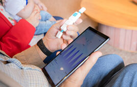
Coleman’s team at UC San Diego has been working in medical settings for four years. Their sensors have been used to monitor premature babies, pregnant women, patients in Intensive Care Units, and patients suffering from sleep disorders.
Coleman and colleagues quickly found out that nurses wanted the sensors to come in a peel-and-stick form, like a medical-grade Band Aid. The medium on which the sensors were placed also needed to be FDA-approved.
The sensors’ original fabrication process involved 10 steps — five of which had to take place in a cleanroom. Also, the steps to remove the sensors from the silicon wafer they’re built on alone took anywhere from 10 to 20 minutes. And the sensors remained fragile and susceptible to rips and tears.
But what if you could use the adhesive properties of a Band Aid-like medium to help peel off the sensors from the silicon wafer easily and quickly? Wouldn’t that make the process much simpler — and faster? That was the question that Dae Kang, a Jacobs School Ph.D. student in Coleman’s research group, set out to answer. The result of his efforts is a process that comprises only six steps — three of them in the cleanroom. The steps that took 10 to 20 minutes before now take just 35 seconds.
Kang created a coating about 20 to 50 micrometers thick, made of a silicon-like material called an elastomer, to easily remove the sensors, made of gold and chromium, from the silicon wafer. This was tricky work. The coating had be sticky enough to allow researchers to build the sensors in the first place, but loose enough to allow them to peel off the wafer.
“It’s a Goldilocks problem,” Coleman says.
The new process doesn’t require any chemical solvents. That means the sensors can be peeled off with any kind of adhesive, from scotch tape to a lint roller, as researchers demonstrated in the study.
Coleman’s team also showed that the sensors could be fabricated on a curved, flexible film typically used to manufacture flexible printed circuits and the outside layer of spacesuits. Researchers were able to easily peel off the sensors from the curved film without compromising their functioning.
In order to make the sensors more like peel-off stickers, researchers essentially had to build the sensors upside down so that their functioning part would be exposed after they were removed from the wafer. This was key to allow for easy processing with a single peel-off step.
Researchers also demonstrated that the sensors they built with the new fabrication process were functional. They placed a sensor on a subject’s forehead and hooked it up to an electroencephalography machine. The sensors were able to detect a special brain signal present only when the subject’s eyes were closed — a classic electroencephalogram testing procedure. The researchers also demonstrated that these sensors are able to detect other electrical rhythms of the body, such as the heart’s electrical activity detected during an electro-cardiogram or EKG.
Release Date: October 27, 2015
Source: UC San Diego