Research & Development World

  • R&D World Home
  • Topics
    • Aerospace
    • Automotive
    • Biotech
    • Careers
    • Chemistry
    • Environment
    • Energy
    • Life Science
    • Material Science
    • R&D Management
    • Physics
  • Technology
    • 3D Printing
    • A.I./Robotics
    • Software
    • Battery Technology
    • Controlled Environments
      • Cleanrooms
      • Graphene
      • Lasers
      • Regulations/Standards
      • Sensors
    • Imaging
    • Nanotechnology
    • Scientific Computing
      • Big Data
      • HPC/Supercomputing
      • Informatics
      • Security
    • Semiconductors
  • R&D Market Pulse
  • R&D 100
    • 2025 R&D 100 Award Winners
    • 2025 Professional Award Winners
    • 2025 Special Recognition Winners
    • R&D 100 Awards Event
    • R&D 100 Submissions
    • Winner Archive
  • Resources
    • Research Reports
    • Digital Issues
    • Educational Assets
    • Subscribe
    • Video
    • Webinars
    • Content submission guidelines for R&D World
  • Global Funding Forecast
  • Top Labs
  • Advertise
  • SUBSCRIBE

Imaging electrons moving at 80,000 m/sec in a semiconductor

By R&D Editors | October 29, 2014

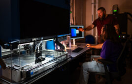
Postdoctoral fellow Keiki Fukumoto, together with researcher Ken Onda and Professor Shinya Koshihara, all of the Graduate School of Science and Engineering at the Tokyo Institute of Technology, succeeded in direct observation and video imaging of electron flow at 80,000 m/sec in a semiconductor. They did so by combining a new laser pulse light source and a photoemission electron microscope (PEEM) to develop an ultra high-speed microscope that enabled visualization of electrons on a 20 nm and 200 femtosec scale.

Semiconductors are widely used in PCs, mobile phones and solar batteries, and have become indispensable, but there had been no method to view the movement of the carriers (electrons) that controlled their behavioral functions.

With the advance of the nano-sizing of semiconductor elements, attention is on the development of elements (transistors, solar batteries, LEDs, quantum computers) that use the resulting quantum size effect. Devices able to visually assess that electrical conductivity are expected to have a major impact on future semiconductor element development.

The results of this research were published in the online bulletin version of the American scientific journal “Applied Physics Letters” on March 7.

Direct imaging of electron recombination and transport on a semiconductor surface by femtosecond time-resolved photoemission electron microscopy

Source: Tokyo Institute of Technology

Time-resolved PEEM video imagery of electron movement. (a): Outline of measurement method. (b)&(c): Photoelectron microscope images after laser irradiation at 20ps and 40ps. (d)&(e): Magnifications of the center areas of (b)&(c). (f): Electron movement can be confirmed from the vertical-direction profiles in (d)&(e). Fig. 2: (a),(b),(c) are the movement ranges for electrons plotted against time using the electric field gradient between different electrodes (voltage value ÷ electrode interval). The movement speed of the electrons is calculated from the linear fit inclination. (d) is electron movement speed plotted against the electric field gradient.

Related Articles Read More >

New metal-organic material can capture water from atmosphere
Sandia scientists develop rapid PFAS test using desorption electrospray ionization 
Colored scanning electron microscopy image showing multiple high-index-facet high-entropy alloy nanoparticles. Image courtesy of Northwestern.
Northwestern unravels a key surface-control problem in high-entropy alloy catalysts
The cloud Is democratizing atomistic simulation, but advantage still comes from execution
rd newsletter
EXPAND YOUR KNOWLEDGE AND STAY CONNECTED
Get the latest info on technologies, trends, and strategies in Research & Development.

R&D World Digital Issues

Fall 2025 issue

Browse the most current issue of R&D World and back issues in an easy to use high quality format. Clip, share and download with the leading R&D magazine today.

R&D 100 Awards
Research & Development World
  • Subscribe to R&D World Magazine
  • Sign up for R&D World’s newsletter
  • Contact Us
  • About Us
  • Drug Discovery & Development
  • Pharmaceutical Processing
  • Global Funding Forecast

Copyright © 2026 WTWH Media LLC. All Rights Reserved. The material on this site may not be reproduced, distributed, transmitted, cached or otherwise used, except with the prior written permission of WTWH Media
Privacy Policy | Advertising | About Us

Search R&D World

  • R&D World Home
  • Topics
    • Aerospace
    • Automotive
    • Biotech
    • Careers
    • Chemistry
    • Environment
    • Energy
    • Life Science
    • Material Science
    • R&D Management
    • Physics
  • Technology
    • 3D Printing
    • A.I./Robotics
    • Software
    • Battery Technology
    • Controlled Environments
      • Cleanrooms
      • Graphene
      • Lasers
      • Regulations/Standards
      • Sensors
    • Imaging
    • Nanotechnology
    • Scientific Computing
      • Big Data
      • HPC/Supercomputing
      • Informatics
      • Security
    • Semiconductors
  • R&D Market Pulse
  • R&D 100
    • 2025 R&D 100 Award Winners
    • 2025 Professional Award Winners
    • 2025 Special Recognition Winners
    • R&D 100 Awards Event
    • R&D 100 Submissions
    • Winner Archive
  • Resources
    • Research Reports
    • Digital Issues
    • Educational Assets
    • Subscribe
    • Video
    • Webinars
    • Content submission guidelines for R&D World
  • Global Funding Forecast
  • Top Labs
  • Advertise
  • SUBSCRIBE