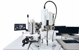
 JEOL, developer of cutting-edge electron microscopes for materials characterization and analysis, introduces its latest SEM, the JSM-IT510. This new Scanning Electron Microscope (SEM) features productivity-enhancing automation, including “Simple SEM” automated imaging, automated montaging (both image and EDS map) and live EDS analysis (spectrum and map).
The IT510 is the successor to the popular JEOL IT500 InTouchScope SEM, with its large sample chamber and tungsten or LaB6 filament. The IT510 features JEOL Intelligent Technology that enables seamless navigation from optical to SEM imaging, Live EDS and 3D analysis, and auto functions from alignment to focus for fast, clear and sharp images.
The user of the new IT510 has several productivity-enhancing new features:
- The new Simple SEM function automates image collection at multiple locations on a sample, and sets the various conditions required, including magnification and settings. Simple SEM simplifies and automates workflow for routine tasks.
- A new “Live 3D” function constructs 3D images of the sample surface during observation showing surface shape and depth information in real time.
- A Signal Depth automated function calculates the X-ray generation depth to support understanding of the analytical spatial resolution within a specimen under the conditions set. Useful when conducting elemental analysis.
- A new Low-vacuum Hybrid Secondary Electron Detector collects both electron and photon signals, providing an image with high S/N and enhanced topographic information. This detector also supports photon imaging with specimens that give a cathodoluminescence response.
- Live Mapping displays the elemental map simultaneously with SEM imaging, made possible by a new Integrated SEM and Energy Dispersive X-ray Spectrometer (EDS) System. The user can switch seamlessly between the live map view and spectrum view during SEM image observation. Then they can overlay the element maps of interest on the live SEM image for enhancing understanding of element distribution within a specimen.
- Zeromag software seamlessly navigates to the area of interest from an optical image of a larger general area of the sample. The user is never lost and can easily navigate to the desired observation area by simply clicking on the optical image.
The JEOL IT510 is designed for unprecedented ease-of-use with advanced SEM technology in a compact platform. This smart-flexible-powerful Scanning Electron Microscope delivers the highest level of intelligent technology with built-in automation for the most versatile analytical SEM available today.


Tell Us What You Think!