Research & Development World

  • R&D World Home
  • Topics
    • Aerospace
    • Automotive
    • Biotech
    • Careers
    • Chemistry
    • Environment
    • Energy
    • Life Science
    • Material Science
    • R&D Management
    • Physics
  • Technology
    • 3D Printing
    • A.I./Robotics
    • Software
    • Battery Technology
    • Controlled Environments
      • Cleanrooms
      • Graphene
      • Lasers
      • Regulations/Standards
      • Sensors
    • Imaging
    • Nanotechnology
    • Scientific Computing
      • Big Data
      • HPC/Supercomputing
      • Informatics
      • Security
    • Semiconductors
  • R&D Market Pulse
  • R&D 100
    • Call for Nominations: The 2025 R&D 100 Awards
    • R&D 100 Awards Event
    • R&D 100 Submissions
    • Winner Archive
    • Explore the 2024 R&D 100 award winners and finalists
  • Resources
    • Research Reports
    • Digital Issues
    • R&D Index
    • Subscribe
    • Video
    • Webinars
  • Global Funding Forecast
  • Top Labs
  • Advertise
  • SUBSCRIBE

Nano-Calligraphy on Graphene

By University of Manchester | December 8, 2016

Credit: University of Manchester

Scientists at The University of Manchester and Karlsruhe Institute of Technology have demonstrated a method to chemically modify small regions of graphene with high precision, leading to extreme miniaturisation of chemical and biological sensors.

Writing in ACS Applied Materials & Interfaces by researchers led by  Aravind Vijayaraghavan, Ph.D., show that it is possible to combine graphene with chemical and biological molecules and form patterns, which are 100s of nanometres wide.

Graphene is the world’s first two-dimensional material. It is strong, transparent, flexible and the world’s most conductive material. Every atom in graphene is exposed to its environment, allowing it to sense changes in its surroundings.

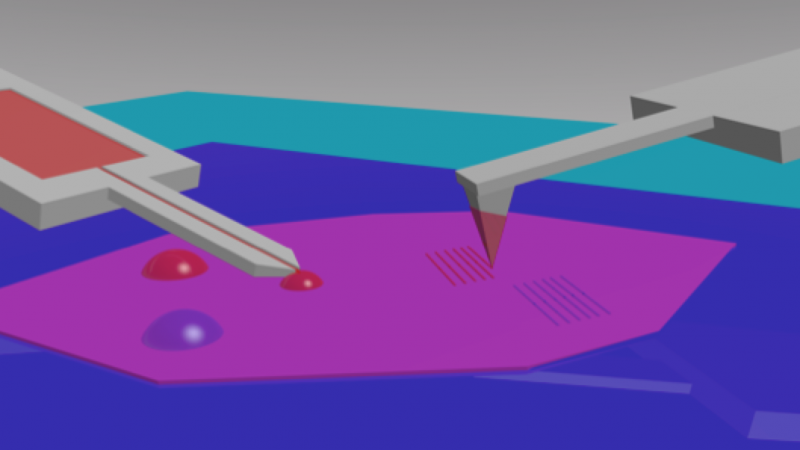
Using technology that resembles writing with a quill or fountain pen, the scientists were able to deliver chemical droplets to the surface of graphene in very small volumes. In order to achieve such fine chemical patterns, the researchers used droplets of chemicals less than 100 attolitres (10-16 L) in volume.

These techniques are key to enabling graphene sensors which can be used in real-world applications; graphene sensors fabricated this way have the potential to be used in blood tests, minimising the amount of blood a patient is required to give.

Dr. Vijayaraghavan explained: “Two types of ‘pens’ were used, one which is dipped into the reactive ‘ink’ like a quill to cover the nib, and the other where the ink is filled into a reservoir and flows through a channel in the nib, just like in a fountain pen. An array of such micro-pens are moved over the graphene surface to deliver the chemical droplets which react with the graphene. The first method is known as Dip-Pen Nanolithography (DPN) and the latter is known as Microchannel Cantilever Spotting (µCS).”

Dr. Michael Hirtz, co-investigator from Karlsruhe added: “By chemically modifying the graphene in such small regions, we can develop chemical and biological sensors which only require very small volumes of fluid to detect various constituents. This, combined with the high sensitivity of graphene sensors, leads us to imagine that in the future we could perform a full blood test on a patient with just one tiny drop of blood, instead of a full syringe.”


Related Articles Read More >

Floating solar mats clean polluted water — and generate power
Nanodots enable fine-tuned light emission for sharper displays and faster quantum devices
New photon-avalanching nanoparticles could enable next-generation optical computers
New “nose-computer interface” aims to upgrade Rover’s nose for better drug detection methods
rd newsletter
EXPAND YOUR KNOWLEDGE AND STAY CONNECTED
Get the latest info on technologies, trends, and strategies in Research & Development.
RD 25 Power Index

R&D World Digital Issues

Fall 2024 issue

Browse the most current issue of R&D World and back issues in an easy to use high quality format. Clip, share and download with the leading R&D magazine today.

Research & Development World
  • Subscribe to R&D World Magazine
  • Enews Sign Up
  • Contact Us
  • About Us
  • Drug Discovery & Development
  • Pharmaceutical Processing
  • Global Funding Forecast

Copyright © 2025 WTWH Media LLC. All Rights Reserved. The material on this site may not be reproduced, distributed, transmitted, cached or otherwise used, except with the prior written permission of WTWH Media
Privacy Policy | Advertising | About Us

Search R&D World

  • R&D World Home
  • Topics
    • Aerospace
    • Automotive
    • Biotech
    • Careers
    • Chemistry
    • Environment
    • Energy
    • Life Science
    • Material Science
    • R&D Management
    • Physics
  • Technology
    • 3D Printing
    • A.I./Robotics
    • Software
    • Battery Technology
    • Controlled Environments
      • Cleanrooms
      • Graphene
      • Lasers
      • Regulations/Standards
      • Sensors
    • Imaging
    • Nanotechnology
    • Scientific Computing
      • Big Data
      • HPC/Supercomputing
      • Informatics
      • Security
    • Semiconductors
  • R&D Market Pulse
  • R&D 100
    • Call for Nominations: The 2025 R&D 100 Awards
    • R&D 100 Awards Event
    • R&D 100 Submissions
    • Winner Archive
    • Explore the 2024 R&D 100 award winners and finalists
  • Resources
    • Research Reports
    • Digital Issues
    • R&D Index
    • Subscribe
    • Video
    • Webinars
  • Global Funding Forecast
  • Top Labs
  • Advertise
  • SUBSCRIBE