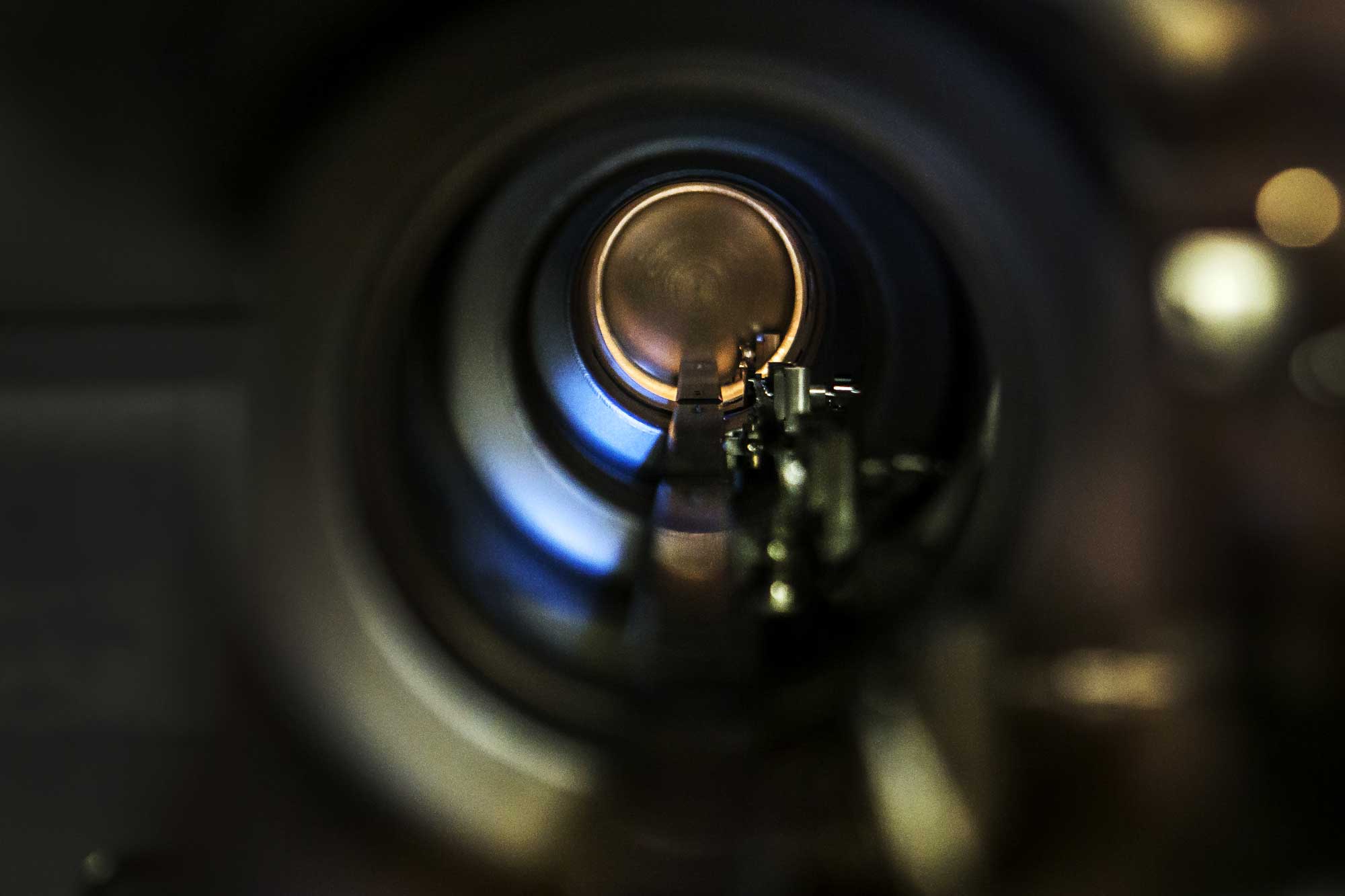
The main growth chamber of the molecular epitaxy beam apparatus used to make the nanoparticle-infused gallium nitride semiconductors. The semiconductors could boost LED efficiency by up to 50 percent, and even lead to invisibility cloaking devices. Image credit: Joseph Xu, Michigan Engineering
Invisibility cloaks may be on the way with the addition of metallic nanoparticles to semiconductors.
Researchers from the University of Michigan created a new technique that could improve the efficiency of LED lighting by 50 percent while adding no cost during manufacturing. In addition, the new technique could enable cloaks that render objects partially invisible by inducing a phenomenon called reverse refraction, where light waves bend backwards in a way that doesn’t occur in nature, potentially directing them around an object or away from the eye.
The research team integrated nanoparticles with the molecular beam epitaxy process used to make semiconductors by spraying multiple layers of metallic elements onto a wafer to create exactly the right conductive properties for a given purpose.
Next, the scientists applied an ion beam between the layers to push metal out of the semiconductor wafer and onto the surface.
Controlling the size and placement of the nanoparticles was done by varying the angle and intensity of the ion beam. Applying the ion beam over and over between each layer created a semiconductor with the nanoparticles interspersed throughout.
“If you carefully tailor the size and spacing of nanoparticles and how deeply they’re embedded, you can find a sweet spot that enhances light emissions,” Myungkoo Kang, a former graduate student in Goldman’s lab and first author on the study, said in a statement. “This process gives us a much simpler and less expensive way to do that.”
Metal nanoparticles increase LED efficiency by acting as tiny antennas that alter and redirect the electricity running through the semiconductor, turning more of it into light. The nanoparticles also assist in reflecting light out of the device, preventing it from being trapped inside and wasted.
The process can be used with gallium nitride—which is used in LED lighting—and also can boost the efficiency in other semiconductor products including solar cells.
“This is a seamless addition to the manufacturing process and that’s what makes it so exciting,” Rachel Goldman, University of Michigan professor of materials science and engineering and physics, said in a statement. “The ability to make 3D structures with these nanoparticles throughout is going to open a lot of possibilities.”
Previous attempts to incorporate nanoparticles to LED lighting have been unsuccessful and impractical for large-scale manufacturing. They have also focused on more expensive metals including silver, gold and platinum.
Successfully adding nanoparticles to metal entails precision because additional and expensive manufacturing steps are often required and there is no cost-effective method to incorporate particles below the surface.
“From the very early days of semiconductor manufacturing, the goal was always to spray a smooth layer of elements onto the surface,” Goldman said. “If the elements formed particles instead, it was considered a mistake.
“But we realized that those ‘mistakes’ are very similar to the particles that manufacturers have been trying so hard to incorporate into LEDs,” she added. “So we figured out a way to make lemonade out of lemons.”
By carefully sizing and spacing an array of nanoparticles, scientists may be able to induce and control reverse refraction in specific wavelengths of light.
“For invisibility cloaking, we need to both transmit and manipulate light in very precise ways, and that’s very difficult today,” Goldman said. “We believe that this process could give us the level of control we need to make it work.”


