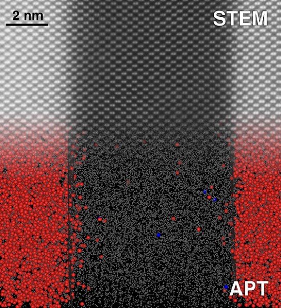
An aberration-correction algorithm (bottom) makes atom probe tomography (APT) on par with scanning transmission electron microscopy (STEM) (top)—an industry standard—for characterizing impurities in semiconductors and their interfaces. STEM images are averages over many atoms in a column, while APT shows the position of individual atoms and can determine their elemental makeup. Credit: Jonathan Poplawsky and Jason Smith, Oak Ridge National Laboratory
The Science
What if we could make a powerful scientific tool even better? Atom probe tomography (APT) is a powerful way of measuring interfaces on a scale comparable to the distance between atoms in solids. It also has a chemical sensitivity of less than 10 parts per million. However, it doesn’t work as well as it could. Scientists applied “electron glasses” to correct aberrations in APT data. Now, researchers have an extremely accurate, precise method for measuring the distances between interfaces in vital semiconductor structures. These structures include a silicon (Si) layer sandwiched by a silicon germanium alloy (SiGe).
The Impact
If it contains a computer or uses radio waves, it relies on a semiconductor. To make better semiconductors, scientists need better ways to analyze the interfaces involved. This new APT approach offers a precise, detailed view of the interface between Si and SiGe. It offers data to optimize interfacial integrity. Improved knowledge of the interfaces is key to advancing technologies that employ semiconductors.
Summary
As electronic devices shrink, more precise semiconductor synthesis and characterization are needed to improve these devices. APT can identify atom positions in 3-D with sub-nanometer resolution from detected evaporated ions, and can detect dopant distributions and low-level chemical segregation at interfaces; however, until now, aberrations have compromised its accuracy. Factors affecting the severity of aberrations include the sequence from which the interface materials are evaporated (for example, SiGe to Si versus Si to SiGe) and the width of the needle-shaped sample from which material is evaporated (for example, the larger the amount of material analyzed, the greater the aberrations). There are several advantages to understanding the sub-nanometer-level chemical make-up of a material with APT. For example, APT is 100 to 1,000 times more chemically sensitive than the traditional interface measurement technique, scanning transmission electron microscopy (STEM). Moreover, because APT is a time-of-flight, secondary ion mass spectrometry method, it is superior for detecting lightweight dopants and dopants with similar atomic numbers as the bulk, such as phosphorus in Si. In this experiment, researchers at Oak Ridge National Laboratory and HRL Laboratories, LLC assessed the ability of APT to accurately measure SiGe/Si/SiGe interfacial profiles by comparing APT results to those of optimized atomic-resolution STEM measurements from the same SiGe/Si/SiGe sample. Without applying a post-APT reconstruction processing method, the measured Si/SiGe interfacial widths between APT and STEM datasets match poorly. Aberrations create density variations in the APT dataset that do not exist in the material.pplied an algorithm to correct density variations normal to the interface (that is, in the z-direction) of the APT data, which resulted in accurate interfacial profile measurements. Scientists can use this accurate method for characterizing SiGe/Si/SiGe interfacial profiles to consistently measure the same interface width with a precision close to 1 Angstrom (that is, a fraction of the distance between two atoms). This knowledge may be used to improve many semiconductor devices with Si/SiGe or similar interfaces.
Funding
Atom probe tomography and scanning transmission electron microscopy were conducted at the Center for Nanophase Materials Sciences, a Department of Energy Office of Science user facility.
Publications
O. Dyck, D.N. Leonard, L.F. Edge, C.A. Jackson, E.J. Pritchett, P.W. Deelman, and J.D. Poplawsky, “Accurate quantification of Si/SiGe interface profiles via atom probe tomography.” Advanced Materials Interfaces 4(21),1700622 (2017). [DOI: 10.1002/admi.201700622]