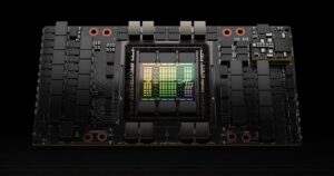
H100 image [NVIDIA]
Buried in its Q3 earnings call was the real news: Nvidia and TSMC produced the first Blackwell wafers on American soil.
“We remain focused on building resiliency and redundancy in our global supply chain. Last month, in partnership with TSMC, we celebrated the first Blackwell wafer produced on US soil,” said Colette Kress, the company’s CFO. “We will continue working with Foxconn, Wistron, Amkor, SPIL and others to expand our presence in the U.S. over the next four years.”
Nvidia reported $57 billion in revenue, guided $65 billion for Q4, and sent the stock up 3% after hours on Nov. 19, 2025. While analysts fixated on margins, China restrictions, and whether the AI “bubble” is dead, they missed the industrial signal.
The manufacturing news marks the first time a flagship AI GPU at TSMC’s 4nm-class node has ever started wafers in the U.S. TSMC Arizona Fab 21 just proved it can yield the most complex, highest-value silicon on earth on American soil.
Nvidia is duplicating the entire backend supply chain in U.S. facilities: advanced packaging (CoWoS, InFO), OSAT, test, and final assembly. The goal is explicit: eliminate single-point failure in Taiwan when export controls have already severed the China market.
Kress was clear on the immediate financial impact: “Sizable purchase orders never materialized in the quarter due to geopolitical issues… we are not assuming any data center compute revenue from China” in the Q4 outlook.
Jensen Huang was blunter: “To establish a sustainable leadership and position in AI computing, America must win. [It must have] the support of every developer, and be the platform of choice for every commercial business including those in China.” Yet he kept the door ajar to selling GPUs to China with the goal of supporting the developer ecosystem.
This duality, manufacturing onshoring coupled with ecosystem diplomacy, paints a complex picture for the future of R&D. While Huang refuses to cede the Chinese market entirely, the technical reality is that the hardware roadmap has bifurcated. The “cutting edge” (Blackwell and the upcoming Rubin platform) is being physically ring-fenced in the U.S. supply chain, while the Chinese market is relegated to compliant silicon to keep the CUDA software platform alive.
For the U.S. engineering community, the heavy lifting is coming home. Kress’s mention of partners like Amkor and Wistron is the signal. A wafer printed in Arizona is useless without advanced packaging, specifically Chip-on-Wafer-on-Substrate (CoWoS), which has historically been the bottleneck in Taiwan.
By committing to expand these partnerships in the U.S. “over the next four years,” Nvidia is effectively underwriting the buildout of a domestic advanced packaging ecosystem. This moves the challenge from a “shipping” problem to a “process engineering” problem for American firms. The question is no longer if the U.S. can manufacture the leading edge, but if it can replicate TSMC’s legendary yields and packaging precision outside of the Hsinchu Science Park.
The race is officially on. For R&D leaders in semiconductor manufacturing, materials science, and industrial automation, the coming years will be about proving these systems can be built, packaged, and shipped entirely within American borders.
As Huang noted regarding the Blackwell ramp: “The world doesn’t have an excess of anything to squander.” That now applies to U.S. engineering talent as much as it does to megawatts.