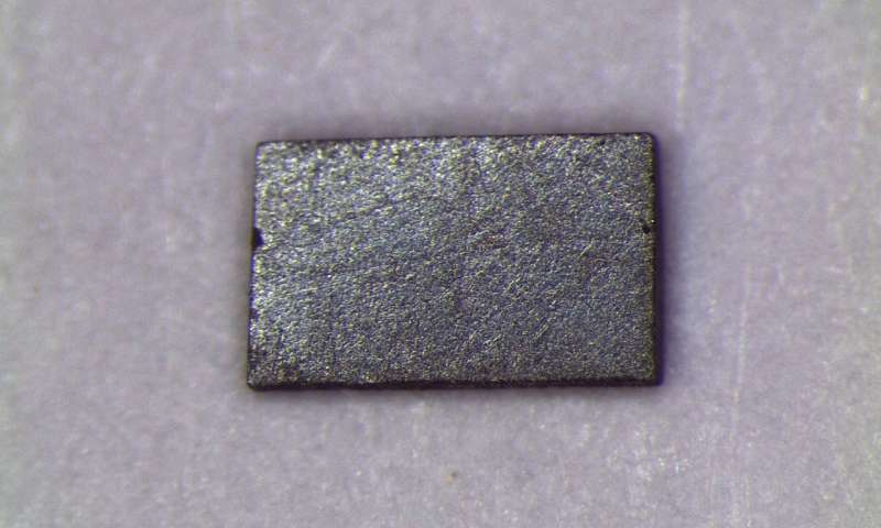
Pictured is a crystal of ytterbium dodecaboride, or YbB 12. Credit: University of Michigan
Quantum materials are a type of odd substance that could be many times more efficient at conducting electricity through our iPhones than the commonly used conductor silicon—if only physicists can crack how the stuff works.
A University of Michigan physicist has gotten one step closer with detailing a novel quantum material, ytterbium dodecaboride, or YbB12, and imaging how efficiently electricity is conducted through this material. The demonstration of this material’s conductivity will help contribute to scientists’ understanding of the spin, charge, and energy flow in these electromagnetic materials.
YbB12 is a very clean crystal that is unusual in it shares the properties of both conductors and insulators. That is, the bulk interior of YbB12 is an insulator and doesn’t conduct electricity, while its surface is extraordinarily efficient at conducting electricity. But researchers needed to be able to measure exactly how good at conducting electricity this material is.
“Right now, we are using a phone to talk. Inside the phone are its key parts: a transistor made of silicon that passes electricity through the device,” said project leader Lu Li, U-M associate professor of physics. “These silicon semiconductors use the bulk of their own material to make a path for electric current. That makes it difficult to make electronic devices faster or more compact.”
Replacing a phone’s silicon transistors with ones made of quantum materials would make the phone much faster—and much lighter. That’s because the transistors inside the device would conduct electricity very quickly on their surfaces, but could be made much smaller, with a lighter core beneath a layer of the metal’s insulating interior.
Quantum materials would not be limited to powering our phones. They could be used in quantum computing, a field still in its infancy, but which could be used for cybersecurity. Our computers currently work by processing data in binary digits: 0 and 1. But there’s a limit to how fast computers can process data in this way. Instead, quantum computers would use the quantum properties of atoms and electrons to process information, opening up the ability to process huge volumes of information much faster.
Li studied YbB12 to understand the material’s electronic signature, which tells researchers how well a material conducts electricity. In a clean metal that conducts electricity very efficiently, electrons form clusters within the metals.
The swings of these clusters lead to oscillations of the electrical resistance of the material. This oscillation tells researchers how efficiently the material is able to conduct electricity. In this study, Li was able to measure the oscillation of resistance of a bulk insulator, a problem he’s been trying to solve for four years.
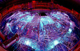
To measure this oscillation, Li used a very powerful magnet located in a lab at the National High Magnetic Field Laboratory in Florida. This magnet is similar to a magnet you would use to fix a photo to your refrigerator, says Li, but many times more powerful. A fridge magnet has a pull of about 0.1 Tesla, a unit of measurement for the magnetic field. The magnet at the Florida laboratory has a pull of 45 Tesla. That’s about 40 times more powerful than the magnet used in an MRI machine.
To measure the efficiency of YbB12, Li ran an electric current through the sample in the presence of the magnet. Then, he examined how much the electric voltage dropped throughout the sample. That told Li how much resistance was present in the material.
“We finally got the right evidence. We found a material that was a good insulator on its interior, but at its surface was a good conductor—so good that we can make an electric circuit on that conductor,” Li said. “You can imagine that you can have a circuit that moves as fast as imaginable on a teeny, tiny surface. That’s what we hope to achieve for future electronics.”