Imagine pointing your smartphone at a salty snack you found at the back of your pantry and immediately knowing if its ingredients had turned rancid.
Devices called spectrometers can detect dangerous chemicals based on a unique “fingerprint” of absorbed and emitted light. But these light-splitting instruments have long been both bulky and expensive, preventing their use outside the lab.
Until now.
Engineers at the University of Wisconsin-Madison have developed a spectrometer that is so small and simple that it could integrate with the camera of a typical cell phone without sacrificing accuracy.
The researchers published a description of the devices March 4, 2019, in the journal Nature Communications.
“This is a compact, single-shot spectrometer that offers high resolution with low fabrication costs,” says Zhu Wang, who was the first author on the paper.
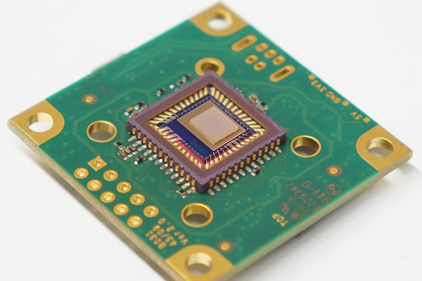
New compact and low-cost devices could help turn ordinary cell phones into advanced analytical tools. Image: Courtesy of Zongfu Yu
The team’s devices also have an advanced capability called hyperspectral imaging, which collects information about each individual pixel in an image order to identify materials or detect specific objects amidst a complicated background. Hyperspectral sensing, for example, could be used to detect seams of valuable minerals within rock faces or to identify specific plants in a highly vegetated area.
Every element’s spectral fingerprint includes unique emitted or absorbed wavelengths of light—and the spectrometer’s ability to sense that light is what has enabled researchers to do everything from analyze the composition of unknown compounds to reveal the makeup of distant stars.
Spectrometers usually rely on prisms or gratings to split light emitted from an object into discrete bands—each corresponding to a different wavelength. A camera’s photodetector can capture and analyze those bands; for example, the spectral fingerprint of the element sodium consists of two bands with wavelengths of 589 and 590 nanometers.
Human eyes see 590-nanometer wavelength light as a yellowish-orange shade. Shorter wavelengths correspond to blues and purples, whereas longer wavelengths appear red. Sunlight contains a complete rainbow mixed together, which we see as white.
To resolve the difference among a mixture of different colors, spectrometers usually must be relatively large with a long path length for light beams to travel and separate.
Yet the team created tiny spectrometers, measuring just 200 micrometers on each side (roughly one-20th the area of a ballpoint pen tip) and delicate enough to lie directly on a sensor from a typical digital camera.
That small size was possible because the researchers based their device on specially designed materials that forced incoming light to bounce back and forth several times before reaching the sensor. Those internal reflections elongated the path along which light traveled without adding bulk, boosting the devices’ resolution.
And the devices performed hyperspectral imaging, resolving two distinct images (of the numbers five and nine) from a snapshot of an overlaid projection that combined the pair into something indistinguishable to the naked eye.
Now the team hopes to boost the device’s spectral resolution as well as the clarity and crispness of the images it captures. Those improvements could pave the way for even more enhanced sensors.
A National Science Foundation CAREER Award and DARPA Young Faculty Award (YFA) supported the research. The paper’s senior author was Dugald C. Jackson Assistant Professor and Vilas Associate Zongfu Yu, in the Department of Electrical and Computer Engineering. Other collaborators at UW-Madison included Assistant Professor Mikhail Kats, Soongyu Yi, Ang Chen, Ming Zhou, Graham Joe, Alireza Shahsafi. Additionally, Ken Xingze Wang at Huazhong University of Science and Technology as well as Ting Shan Luk, Anthony James, John Nogan and Willard Ross at Sandia National Laboratories contributed to the research.