Research & Development World

  • Home Page
  • Topics
    • Aerospace
    • Archeology
    • Automotive
    • Biotech
    • Chemistry
    • COVID-19
    • Environment
    • Energy
    • Life Science
    • Material Science
    • R&D Market Pulse
    • R&D Management
    • Physics
  • Technology
    • 3D Printing
    • A.I./Robotics
    • Battery Technology
    • Controlled Environments
      • Cleanrooms
      • Graphene
      • Lasers
      • Regulations/Standards
      • Sensors
    • Imaging
    • Nanotechnology
    • Scientific Computing
      • Big Data
      • HPC/Supercomputing
      • Informatics
      • Security
      • Software
    • Semiconductors
  • 2021 R&D 100 Award Winners
    • R&D 100 Awards
    • 2020 Winners
    • Winner Archive
  • Resources
    • Digital Issues
    • Podcasts
    • Subscribe
  • Global Funding Forecast
  • Webinars

Researchers Find New Way to 3D Print Electronic Circuits

By Kenny Walter | November 9, 2017

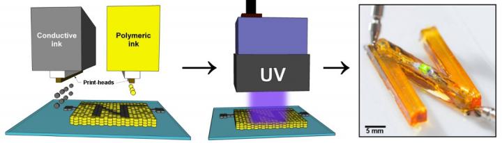
A schematic diagram showing how UV irradiation heats and solidifies conductive and dielectric inks to form the letter N with silver tracks that connect a green LED to a power source. Credit University of Nottingham

Scientists have created a new method to print electronic circuits using a 3D printer.

A team of researchers from the University of Nottingham can now rapidly 3D print fully functional electronic circuits that contain electrically-conductive metallic inks and insulating polymeric inks, which could be useful for medical devices, radio frequency shielding surfaces and novel structures for harvesting solar energy.

“Being able to 3D print conductive and dielectric materials [electrical insulators] in a single structure with the high precision that inkjet printing offers, will enable the fabrication of fully customized electronic components,” Chris Tuck, a professor of Materials Engineering and lead investigator of the study, said in a statement. “You don’t have to select standard values for capacitors when you design a circuit, you just set the value and the printer will produce the component for you.”

The circuits can be produced using a single inkjet printing process where an ultraviolet light rapidly solidifies the inks.

The new method paves the way for the electronics manufacturing industry to produce fully functional components, including 3D antennas and full printed sensors from multiple materials such as metals and plastics.

The researchers combined 2D printed electronics with 3D printing and expanded the impact of Multifunctional Additive Manufacturing—which involves printing multiple materials in a single additive manufacturing system to create components that have broader functionalities.

Existing systems do not typically use more than one material, limiting the functionality of the printed structures. By having two materials like a conductor and an insulator, the researchers expanded the range of functions in electronics.

Using this method, the researchers can create a wristband that includes a pressure sensor and wireless communication circuitry that could be 3D printed and customized for the wearer in a single process.

The new method also speeds up the solidification process of the conductive inks to less than a minute per layer.

“Printing fully functional devices that contain multiple materials in complex, 3D structures is now a reality,” Richard Hague, director of the Centre for Additive Manufacturing (CfAM), said in a statement. “This breakthrough has significant potential to be the enabling manufacturing technique for 21st century products and devices that will have the potential to create a significant impact on both the industry and the public.”

Related Articles Read More >

3D-printed smart wall a cool idea
LLNL optimizes flow-through electrodes for electrochemical reactors with 3D printing
Taking cues from nature, breakthrough ‘cellular fluidics’ technology could have sweeping impacts
Printable Purdue biosensor simultaneously records, makes images of tissues and organs
2021 R&D Global Funding Forecast

Need R&D World news in a minute?

We Deliver!
R&D World Enewsletters get you caught up on all the mission critical news you need in research and development. Sign up today.
Enews Signup

R&D World Digital Issues

February 2020 issue

Browse the most current issue of R&D World and back issues in an easy to use high quality format. Clip, share and download with the leading R& magazine today.

Research & Development World
  • Subscribe to R&D World Magazine
  • Enews Sign Up
  • Contact Us
  • About Us
  • Drug Discovery & Development
  • Pharmaceutical Processing
  • 2022 Global Funding Forecast

Copyright © 2022 WTWH Media LLC. All Rights Reserved. The material on this site may not be reproduced, distributed, transmitted, cached or otherwise used, except with the prior written permission of WTWH Media
Privacy Policy | Advertising | About Us

Search R&D World

  • Home Page
  • Topics
    • Aerospace
    • Archeology
    • Automotive
    • Biotech
    • Chemistry
    • COVID-19
    • Environment
    • Energy
    • Life Science
    • Material Science
    • R&D Market Pulse
    • R&D Management
    • Physics
  • Technology
    • 3D Printing
    • A.I./Robotics
    • Battery Technology
    • Controlled Environments
      • Cleanrooms
      • Graphene
      • Lasers
      • Regulations/Standards
      • Sensors
    • Imaging
    • Nanotechnology
    • Scientific Computing
      • Big Data
      • HPC/Supercomputing
      • Informatics
      • Security
      • Software
    • Semiconductors
  • 2021 R&D 100 Award Winners
    • R&D 100 Awards
    • 2020 Winners
    • Winner Archive
  • Resources
    • Digital Issues
    • Podcasts
    • Subscribe
  • Global Funding Forecast
  • Webinars