Contamination on devices such as semiconductors and disk drive components poses a serious risk for reduced yield and reliability. In many industries there is a general attitude that some loss is acceptable, resulting in billions of dollars of lost revenue every year. The authors contend that this loss is not inevitable, but rather can be reduced or eliminated through careful but basic contamination and static control policies and procedures.
The physics of electrostatically driven micro-contamination becomes more important as feature size shrinks and “killer” particle size shrinks with it. Proper material selection, airflow control, tool qualification, particle control, and static charge reduction through ionization will reduce and even eliminate defect density and yield loss due to contamination induced defects.
Contamination issues in hi-tech manufacturing
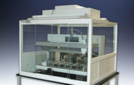
Micro-contamination in high technology manufacturing can be a significant source of yield and reliability loss. For instance, a particle on the surface of a wafer being exposed during a photolithography operation will create a shadow that prints in the subsequent step. If that particle is larger than half of the feature size of the process (Critical Dimension — CD), the die with the particle on its surface will likely be non-functioning. In photolithography one particle destroys one component, but in other steps perhaps one particle can destroy a component roughly 25 percent of the time. The state-of-the-art for semiconductor manufacturing today is 14 nm CD. That means that a 7.2 nm particle can kill a die. Compare this to the size of a typical germ (several thousands of nm) or compare it to the size of a virus (several tens of nm) and it becomes clear that the consequences of micro-contamination can be devastating to the profitability of a semiconductor fab. Likewise, similar micro-contamination issues in the hard disk drive industry where particles as small as several tenths of a micron can lodge between the head and magnetic disk, or in many other high technology manufacturing operations, can be devastating.
 The total number of particles landing on a surface in manufacturing can limit the yield and, hence, the profitability of the process. Virtually every semiconductor fab in the world checks each process step frequently in order to validate that the process is working correctly.
Early in the initial qualification of a semiconductor production line, a discussion between the process engineer and his manager frequently occurs. A go/no-go limit is established for tool qualification for an acceptable number of particles per process step, partially based upon previous experience. This limit is part of the process control regimen that is established for the tool. Effectively, this sets an “acceptable yield loss” specification based upon history rather than physics. If that history transpired without static charge control in the tool, the limits will effectively be budgeting in electrostatically driven micro-contamination.
Tools that pass their specification are said to be in specification with respect to micro-contamination. In spite of this declaration, some companies have come to the conclusion that, qualification limits notwithstanding, any reduction of micro-contamination creates an amazingly large increase in profitability. Therefore, the question is not whether there is a micro-contamination problem, but whether it is a good return on investment to pursue any given micro-contamination improvement program. One data set showing the effects of static charge on wafer contamination was published to demonstrate this fact.1 See Figures 1 and 2.

Coulomb’s law states that the electrostatic force acting between two charged objects is directly proportional to the product of the charges and inversely proportional to the square of the distance between the two objects. When considering the impact of this law in a clean environment, one object might be a large planar surface of a charged material such as a tool panel or a product surface, and the other object a charged particle in the environment. This attraction can be circumvented by grounding the surface, but only if it is conductive. In the case of oppositely charged objects, the particle will be attracted to the charged insulating surface. In fact it will accelerate until it comes in contact with the insulating surface, the force increasing dramatically as the distance between the particle and surface is reduced. The charged particle has three forces acting on it — gravitational, aerodynamic, and electrostatic. For electric fields greater than 1,000 volts/cm it has been demonstrated that the dominant force is the electrostatic force.2
This is a point of great concern. In clean environments there are many instances of process-required insulators. These materials can be easily charged to very high levels. Oppositely charged particles in proximity to these items would be attracted to the surfaces, rapidly contaminating them. Even if the surfaces are of the same polarity as the charged particle, the trajectory of the particle will be drawn off of the carefully engineered unidirectional flow direction and become a contamination candidate. Figures 3 and 4 show the difference between the movement of particles on the laminar air flow (Fig. 3) and particles moving in an environment with charged products and charged walls. These figures also demonstrate the importance of a neutral environment, not just a neutral product. In Fig. 4, note the particle clumping.
Effect of particle size
The distribution of particulate sizes tends to follow a 1/X3 defect size distribution.3 Simply stated, this means that if you have a small number of particles at a given size, there will be many more particulates with an order of magnitude reduction in particle diameter. Leading-edge semiconductor manufacturers are currently concentrating on ramping volume production of FinFET chips at the 14 nm technology node; a 7.2 nm diameter particle being roughly at the critical defect size for such a chip. If some of these 14 nm particles in the process environment are charged, they will be attracted to an oppositely charged insulating material on the wafer in which the chips are manufactured. A particulate of the right material landing on the right location of the chip could result in a failed die at electrical test. A small number of charged particles at the critical defect size could result in a very low process limited device yield at final electrical test.
 Electrostatic bonding and cleaning
Numerous studies4, 5 have shown that the implementation of ionization in process environments in which product transits greatly reduces the number of particulates that are added “per wafer pass.” The concept is that reducing the charge levels, both on surfaces and on particulates in the environment, greatly reduces the force of electrostatic attraction and reduces the electrostatic bond of particulates on a product surface, making them easier to remove in subsequent cleaning process steps.
Control of static charge
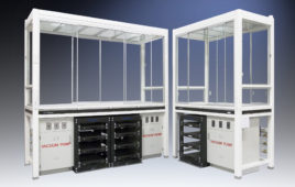
The solutions for solving many of the electrostatic attraction problems are the same as those used for many other static charge issues. Conductive and static dissipative materials should be grounded, which will drain any charge on them. Non-conductive materials are more of a challenge since the electrons within the material will not move, even if the bulk material is connected to ground. The best solution is to engineer the tooling to use conductive or static dissipative materials. Remember that these items must be somehow grounded.
Necessary non-conductive materials (insulators) require more work to make them compatible with static control programs. In some cases they can be coated with films or chemicals to make the surfaces more conductive and less prone to charging. However, care should be taken in using charge suppressing chemicals as they can create problems with chemical outgassing or particulate generation.
Ionization for process required insulators
Charge on process required insulators can also be dealt with through the use of air ionization. Many times, in high airflow cleanrooms, room ionization systems (typically pulsed DC) are already in place. These systems reduce electrostatically induced contamination problems, along with other static control problems. If these systems aren’t in place or don’t provide enough charge control, other ionization systems are available such as steady-state DC ionizing blowers, Alpha emitters, and X-ray generation systems. The selection of the ionizer type needs to be balanced with other critical systems such as cleanliness, airflow, and process issues. Unless a compliance verification procedure already exists for the ionization systems, one must be put in place to ensure the ionization system maintains proper balance and performance over time.
 Contamination and static attraction issues result in yield and reliability losses that have traditionally been considered “a part of doing business.” However, with a relatively simple and reasonable static control program, many of these issues can be resolved and prevented.
References
1. Levit, L.B.; T.M. Hanley; F. Curran. “Watch Out For Electrostatic Attraction.” Solid State Technology. June 2000.
2. Cooper, D.W.; J.J. Wu; M.H. Peters. “Deposition of Sub-micron Aerosol Particles in Integrated Circuit Manufacturing: Experiments.” Journal of Environmental Sciences. 32 (1) pp: 27, 28, 43-45 (1989).
3. Staper, C.H.; R.J. Rosner. “Integrated Circuit Yield Management and Yield Analysis: Development and Implementation.” IEEE Transactions on Semiconductor Manufacturing. Vol. 8, pp. 95-102.
4. Long, C; J. Peterman; L. Levit. “Implementing a Static Control Program to Increase the Efficiency of Wet Cleaning Tools.” MICRO. Jan. 2006.
5. Long, C.W; et al. “A 300-mm Semiconductor Manufacturing Foreign Material Reduction Initiative.” IEEE Transactions on Semiconductor Manufacturing. Vol. 21, Issue 3. Aug. 2008.
Christopher Long is a Senior Engineer with IBM Research. Larry Levit is the owner of LBL Scientific. Carl Newberg is President of MicroStat Laboratories. The authors are all ESD Association members and active Volunteers. www.esda.org
This article appeared in the September/October 2015 issue of Controlled Environments.