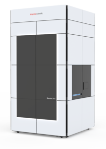
 Thermo Fisher Scientific today unveiled the Thermo Scientific Spectra Ultra, a next-generation scanning transmission electron microscope ((S)TEM) that offers structural and chemical insight on a wide range of materials at atomic-scale resolution.
The new Spectra Ultra provides flexibility to optimize conditions for advanced imaging and analysis in minutes versus hours. To fast-track materials research and improve throughput, users can now rapidly adjust accelerating voltage with high stability. This enables investigation of an extended range of samples, minimizes beam damage and greatly reduces tool optimization overhead.
Spectra Ultra includes a new energy-dispersive X-Ray (EDX) analysis system, the Thermo Scientific Ultra-X, with the largest detector area available in a commercially released (S)TEM. Combined with the new objective lens design, the EDX detector architecture makes it possible to capture X-Rays twice as fast as currently available commercial solutions, allowing the analysis of more beam-sensitive materials and samples with previously undetectably low concentrations of trace elements.
Spectra Ultra builds on the advancements already available in the Thermo Scientific Themis and Spectra platforms, removing complexity so users can obtain quality data at high resolutions.
“The Spectra Ultra, configured with Ultra-X, changes the game for both materials science researchers and semiconductor manufacturers. It can dramatically reduce beam damage by swiftly applying different accelerating voltages, and users will be able to detect light elements with even lower concentration,” said Rosy Lee, vice president of materials science at Thermo Fisher. “In addition, users can quickly image and analyze new and improved materials at increased resolutions, compared to other commercially available solutions.”
“As semiconductor manufacturers approach the physical limits of current process technologies, they are incrementally expanding their use of elements across the periodic table to find solutions that deliver the power, efficiency and performance required for emerging applications,” said Glyn Davies, vice president of semiconductor at Thermo Fisher. “The Spectra Ultra provides industry-leading (S)TEM analysis and characterization capabilities to assist them in meeting the demands for advanced material solutions.”
New features of the Spectra Ultra (S)TEM include:
- A constant power lens and optics design enabling users to rapidly tune the instrument to the optimal voltage for their job.
- The Ultra-X EDX detector which halves the EDX mapping time and elemental concentrations previously undetectable on a commercially released system.
- Increased imaging sensitivity with the ability to measure single electrons, enabling the high-resolution characterization of soft materials.
- Atomic-level analysis for the fundamental development and improvement of materials.
- The optional super high brightness X-CFEG (Cold FEG) emitter that, when combined with the Spectra Ultra, delivers exceptional imaging contrast and analytical capabilities.
These breakthrough technologies expand research possibilities for materials scientists. The minimal electron dose and time needed for EDX enables atomic-level analysis of beam-sensitive specimens. The flexibility to optimize imaging and analytical conditions in a single experiment means faster 3D characterization of both hard and soft materials within one sample, accelerating product development research. With increased throughput and detector collection efficiency, multiuser facilities can offer greater accessibility for a broad variety of projects.
The easy-to-use Spectra Ultra enables semiconductor researchers to analyze devices and structures quickly and more reliably. With the most powerful commercially released EDX system and instant switching of accelerating voltages, the Spectra Ultra facilitates the development of new memory and logic devices at advanced technology nodes.
To learn more about the Thermo Scientific Spectra Ultra (S)TEM, visit thermofisher.com/spectra-ultra.