Research & Development World

  • R&D World Home
  • Topics
    • Aerospace
    • Automotive
    • Biotech
    • Careers
    • Chemistry
    • Environment
    • Energy
    • Life Science
    • Material Science
    • R&D Management
    • Physics
  • Technology
    • 3D Printing
    • A.I./Robotics
    • Software
    • Battery Technology
    • Controlled Environments
      • Cleanrooms
      • Graphene
      • Lasers
      • Regulations/Standards
      • Sensors
    • Imaging
    • Nanotechnology
    • Scientific Computing
      • Big Data
      • HPC/Supercomputing
      • Informatics
      • Security
    • Semiconductors
  • R&D Market Pulse
  • R&D 100
    • 2025 R&D 100 Award Winners
    • 2025 Professional Award Winners
    • 2025 Special Recognition Winners
    • R&D 100 Awards Event
    • R&D 100 Submissions
    • Winner Archive
  • Resources
    • Research Reports
    • Digital Issues
    • Educational Assets
    • Subscribe
    • Video
    • Webinars
    • Content submission guidelines for R&D World
  • Global Funding Forecast
  • Top Labs
  • Advertise
  • SUBSCRIBE

Germanium Outperforms Silicon in Energy-Efficient Transistors with N-und and P-conduction

By TU Dresden | February 23, 2017

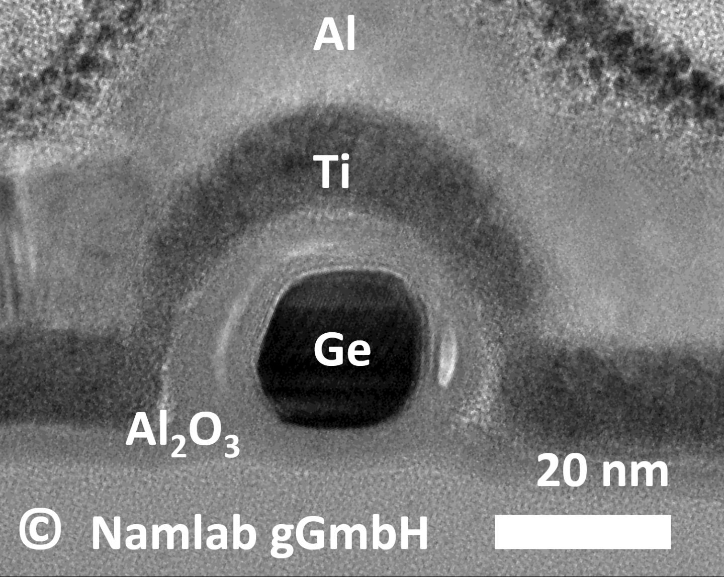
Energy-efficient germanium nanowire transistor with programmable p- and n- conduction is shown. Transmission electron microscope image of cross section. Source: NaMLab gGmbH

A team of scientists from the Nanoelectronic Materials Laboratory (NaMLab gGmbH) and the Cluster of Excellence Center for Advancing Electronics Dresden (cfaed) at the Dresden University of Technology have demonstrated the world-wide first transistor based on germanium that can be programmed between electron- (n) and hole- (p) conduction. Transistors based on germanium can be operated at low supply voltages and reduced power consumption, due to the low band gap compared to silicon. Additionally, the realized germanium based transistors can be reconfigured between electron and hole conduction based on the voltage applied to one of the gate electrodes. This enables to realize circuits with lower transistor count compared to state-of-the-art CMOS technologies.

Today´s digital electronics are dominated by integrated circuits built by transistors. For more than four decades transistors have been miniaturized to enhance computational power and speed. Recent developments aim to maintain this trend by employing materials having higher mobility than silicon in the transistor channel, like germanium and indium-arsenide. One of the limitations in using those materials is the higher static power loss in the transistor´s off-state, also originating from their small band gaps. The scientist team around Jens Trommer and Dr. Walter Weber from NaMLab in cooperation with cfaed succeeded in solving this issue by conceiving the germanium-nanowire transistor with independent gating regions. Dr. Weber who leads cfaed’s Nanowire Research Group points out: “For the first time the results demonstrate the combination of low operation voltages with reduced off-state leakage. The results are a key enabler for novel energy efficient circuits.”

The work has been published in the journal ACS Nano.

Related Articles Read More >

Quantum computing advance: Atom-placed silicon lattice hits 15,000 quantum dots, reveals metal-insulator transition
Lawrence Livermore’s “Science on Saturday” returns, linking computing research with classroom learning
Qunova’s HI-VQE quantum chemistry algorithm is now on AWS Marketplace
Sandia unveils Spectra, a reconfigurable supercomputer for nuclear stockpile simulations
rd newsletter
EXPAND YOUR KNOWLEDGE AND STAY CONNECTED
Get the latest info on technologies, trends, and strategies in Research & Development.

R&D World Digital Issues

Fall 2025 issue

Browse the most current issue of R&D World and back issues in an easy to use high quality format. Clip, share and download with the leading R&D magazine today.

R&D 100 Awards
Research & Development World
  • Subscribe to R&D World Magazine
  • Sign up for R&D World’s newsletter
  • Contact Us
  • About Us
  • Drug Discovery & Development
  • Pharmaceutical Processing
  • Global Funding Forecast

Copyright © 2026 WTWH Media LLC. All Rights Reserved. The material on this site may not be reproduced, distributed, transmitted, cached or otherwise used, except with the prior written permission of WTWH Media
Privacy Policy | Advertising | About Us

Search R&D World

  • R&D World Home
  • Topics
    • Aerospace
    • Automotive
    • Biotech
    • Careers
    • Chemistry
    • Environment
    • Energy
    • Life Science
    • Material Science
    • R&D Management
    • Physics
  • Technology
    • 3D Printing
    • A.I./Robotics
    • Software
    • Battery Technology
    • Controlled Environments
      • Cleanrooms
      • Graphene
      • Lasers
      • Regulations/Standards
      • Sensors
    • Imaging
    • Nanotechnology
    • Scientific Computing
      • Big Data
      • HPC/Supercomputing
      • Informatics
      • Security
    • Semiconductors
  • R&D Market Pulse
  • R&D 100
    • 2025 R&D 100 Award Winners
    • 2025 Professional Award Winners
    • 2025 Special Recognition Winners
    • R&D 100 Awards Event
    • R&D 100 Submissions
    • Winner Archive
  • Resources
    • Research Reports
    • Digital Issues
    • Educational Assets
    • Subscribe
    • Video
    • Webinars
    • Content submission guidelines for R&D World
  • Global Funding Forecast
  • Top Labs
  • Advertise
  • SUBSCRIBE