Research & Development World

  • R&D World Home
  • Topics
    • Aerospace
    • Automotive
    • Biotech
    • Careers
    • Chemistry
    • Environment
    • Energy
    • Life Science
    • Material Science
    • R&D Management
    • Physics
  • Technology
    • 3D Printing
    • A.I./Robotics
    • Software
    • Battery Technology
    • Controlled Environments
      • Cleanrooms
      • Graphene
      • Lasers
      • Regulations/Standards
      • Sensors
    • Imaging
    • Nanotechnology
    • Scientific Computing
      • Big Data
      • HPC/Supercomputing
      • Informatics
      • Security
    • Semiconductors
  • R&D Market Pulse
  • R&D 100
    • 2025 R&D 100 Award Winners
    • 2025 Professional Award Winners
    • 2025 Special Recognition Winners
    • R&D 100 Awards Event
    • R&D 100 Submissions
    • Winner Archive
  • Resources
    • Research Reports
    • Digital Issues
    • Educational Assets
    • Subscribe
    • Video
    • Webinars
    • PharmSci360
    • Content submission guidelines for R&D World
  • Global Funding Forecast
  • Top Labs
  • Advertise
  • SUBSCRIBE

HORIBA launches combined particle size and shape analyzer

By Brian Buntz | August 4, 2026

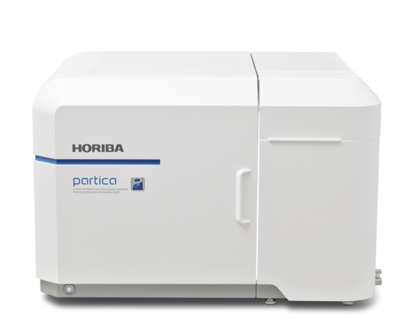
HORIBA Partica laser diffraction and dynamic imaging particle size and shape analyzer

HORIBA’s Partica combines laser diffraction and dynamic image analysis in one instrument. [Image courtesy of HORIBA]

After nearly four decades of developing laser diffraction particle analyzers, HORIBA is repositioning Partica, the brand that has covered its LA-series instruments, around analyzing particle size and shape in a single workflow. The new Partica system combines laser diffraction with dynamic image analysis. HORIBA says the approach gives materials researchers and manufacturers both sets of results in approximately one minute.

HORIBA cites potential applications in a range of sectors, including semiconductors, battery materials, pharmaceuticals, catalysts and other advanced materials. Particles sharing the same nominal diameter can behave differently depending on their shape. In CMP slurries, oversized or agglomerated particles can scratch semiconductor wafers. In battery cathode powders, morphology influences packing density and coating uniformity. In pharmaceutical formulation, it affects dissolution and powder flow.

On the diffraction side, HORIBA specs Partica from 10 nm to 5 mm, with accuracy within ±0.6% of certified reference particle standards. A two-camera dynamic imaging configuration captures shape data from roughly 1 µm up to the millimeter scale, extracting more than 30 parameters including circularity, aspect ratio and Feret diameter. The company also rebuilt the software platform, adding remote operation, automation and data-integrity support.

Tetsuya Mori, HORIBA’s global product line manager, said in a statement that the system supports analyzing pharmaceutical particle characteristics that affect absorption efficiency and speeds evaluation of powder fluidity, “which influences production performance.”

HORIBA released the Partica system globally in March and followed two days later with the CS-900F, a fiber-optic monitor for wet-process chemicals used in semiconductor cleaning and etching. Both fall under Materials & Semiconductor, which generated JPY 156.5 billion of HORIBA’s JPY 333.1 billion in FY2025 sales and is one of three focus fields in the company’s MLMAP2028 plan, which targets JPY 450 billion in group revenue by 2028.
Tell Us What You Think! Cancel reply

You must be logged in to post a comment.

Related Articles Read More >

As AI floods drug discovery with designs, Twist uses DNA chips to tackle the wet-lab bottleneck
How Tecan uses NVIDIA’s BioNeMo Agent Toolkit to flag lab risks before runs fail
Waters targets large, heterogeneous drug modalities with three new mass spectrometry systems
Countable Labs’ CTO Christina Fan on reimagining PCR, one molecule at a time
rd newsletter
EXPAND YOUR KNOWLEDGE AND STAY CONNECTED
Get the latest info on technologies, trends, and strategies in Research & Development.

R&D World Digital Issues

Fall 2025 issue

Browse the most current issue of R&D World and back issues in an easy to use high quality format. Clip, share and download with the leading R&D magazine today.

R&D 100 Awards
Research & Development World
  • Subscribe to R&D World Magazine
  • Sign up for R&D World’s newsletter
  • Contact Us
  • About Us
  • Drug Discovery & Development
  • Pharmaceutical Processing
  • Global Funding Forecast

Copyright © 2026 Arrowfly LLC. All Rights Reserved. The material on this site may not be reproduced, distributed, transmitted, cached or otherwise used, except with the prior written permission of Arrowfly
Privacy Policy | Advertising | About Us

Search R&D World

  • R&D World Home
  • Topics
    • Aerospace
    • Automotive
    • Biotech
    • Careers
    • Chemistry
    • Environment
    • Energy
    • Life Science
    • Material Science
    • R&D Management
    • Physics
  • Technology
    • 3D Printing
    • A.I./Robotics
    • Software
    • Battery Technology
    • Controlled Environments
      • Cleanrooms
      • Graphene
      • Lasers
      • Regulations/Standards
      • Sensors
    • Imaging
    • Nanotechnology
    • Scientific Computing
      • Big Data
      • HPC/Supercomputing
      • Informatics
      • Security
    • Semiconductors
  • R&D Market Pulse
  • R&D 100
    • 2025 R&D 100 Award Winners
    • 2025 Professional Award Winners
    • 2025 Special Recognition Winners
    • R&D 100 Awards Event
    • R&D 100 Submissions
    • Winner Archive
  • Resources
    • Research Reports
    • Digital Issues
    • Educational Assets
    • Subscribe
    • Video
    • Webinars
    • PharmSci360
    • Content submission guidelines for R&D World
  • Global Funding Forecast
  • Top Labs
  • Advertise
  • SUBSCRIBE