Research & Development World

  • R&D World Home
  • Topics
    • Aerospace
    • Automotive
    • Biotech
    • Careers
    • Chemistry
    • Environment
    • Energy
    • Life Science
    • Material Science
    • R&D Management
    • Physics
  • Technology
    • 3D Printing
    • A.I./Robotics
    • Software
    • Battery Technology
    • Controlled Environments
      • Cleanrooms
      • Graphene
      • Lasers
      • Regulations/Standards
      • Sensors
    • Imaging
    • Nanotechnology
    • Scientific Computing
      • Big Data
      • HPC/Supercomputing
      • Informatics
      • Security
    • Semiconductors
  • R&D Market Pulse
  • R&D 100
    • Call for Nominations: The 2025 R&D 100 Awards
    • R&D 100 Awards Event
    • R&D 100 Submissions
    • Winner Archive
    • Explore the 2024 R&D 100 award winners and finalists
  • Resources
    • Research Reports
    • Digital Issues
    • Educational Assets
    • R&D Index
    • Subscribe
    • Video
    • Webinars
  • Global Funding Forecast
  • Top Labs
  • Advertise
  • SUBSCRIBE

Facility Profile: Imec 300mm Cleanroom

By R&D Editors | April 8, 2016

​Imec 300mm Cleanroom, Leuven, Belgium

Cost: €1 billion (USD $1,116,750,000)

Size: 4,000 sm

Team: M+W (construction), Stéphane Beel (architect), and Wim Mertens (responsible for imec’s campus buildings)

Description: Imec’s new 300mm cleanroom is one of the most advanced research facilities in the world dedicated to scaling IC technology beyond 7nm. Its addition now brings imec’s total semiconductor research cleanrooms to 12,000 sm. The facility will be able to serve the entire semiconductor ecosystem, complies with the newest standards in the semiconductor industry, and provides additional space for the most advanced tools that will lead innovations in new device and system concepts.

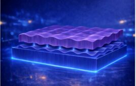
The cleanroom includes a “waffle table’,” a 3-ft. thick concrete slab that forms the basis of the cleanroom. Its structure rests on 831 concrete piles placed 60 feet deep in the ground, making it totally vibration-free and ensuring precision accuracy down to a millionth of a millimeter. The waffle table lies 50 feet above ground and is perforated with no less than 3,300 holes (400 mm diameter), and there is constant air circulation.

To further drive Moore’s Law, crucial innovations are required and imec offers the ideal environment for cost and time effective semiconductor R&D advanced on materials, process steps, modules and novel device concepts for CMOS technologies at least two generations ahead of manufacturing. Imec’s fundamental understanding and ability to bridge the gap between theory and practice will define the new innovations this cleanroom will generate.

Imec’s partners—which includes foundries, IDMs, fabless and fablite companies, equipment and material suppliers—will benefit from the equipment to develop innovative solutions for more powerful, high-performing, cheaper and energy-efficient ICs which are crucial in the evolution of a sustainable digital future. The cleanroom complements imec’s other production facilities including its bio-nanolabs, neuroelectronics labs, imaging and wireless and electronics test labs, photovoltaic pilot lines, and GaN-on-Si, Silicon photonics and MEMS pilot lines.

The cleanroom was constructed by M+W, an internationally renowned contractor of  large-scale high-tech infrastructure. The architecture was designed by Stéphane Beel and includes a reflecting façade which is intended to integrate the building with the environment. Responsible for imec’s campus buildings is Wim Mertens.

The one billion Euro cost comprises both the building and equipment. imec received 100 million euro in funding from the Flemish government and more than 900 million euro in investments from joint R&D partners within the semiconductor industry.

Completion date: The cleanroom opened on March 10, 2016. Installations of the first tools began in January 2016—the project lasted a total of 20 months.

Contact: Hanne Degans, press officer and communications specialist, +32 16 28 17 69, [email protected]  

Related Articles Read More >

First MCU combines gigahertz CPU, 35× faster AI engine and MRAM in single device
Stargate’s $500B bet could force data-center and 1.2 GW grid rethink
Compact AI model lets popular ESP32 microcontroller predict network failures and memory leaks in real time
TSMC’s N3P hits mass production, with N3X customer sampling slated for Q3–Q4 2025a
rd newsletter
EXPAND YOUR KNOWLEDGE AND STAY CONNECTED
Get the latest info on technologies, trends, and strategies in Research & Development.
RD 25 Power Index

R&D World Digital Issues

Fall 2024 issue

Browse the most current issue of R&D World and back issues in an easy to use high quality format. Clip, share and download with the leading R&D magazine today.

Research & Development World
  • Subscribe to R&D World Magazine
  • Enews Sign Up
  • Contact Us
  • About Us
  • Drug Discovery & Development
  • Pharmaceutical Processing
  • Global Funding Forecast

Copyright © 2025 WTWH Media LLC. All Rights Reserved. The material on this site may not be reproduced, distributed, transmitted, cached or otherwise used, except with the prior written permission of WTWH Media
Privacy Policy | Advertising | About Us

Search R&D World

  • R&D World Home
  • Topics
    • Aerospace
    • Automotive
    • Biotech
    • Careers
    • Chemistry
    • Environment
    • Energy
    • Life Science
    • Material Science
    • R&D Management
    • Physics
  • Technology
    • 3D Printing
    • A.I./Robotics
    • Software
    • Battery Technology
    • Controlled Environments
      • Cleanrooms
      • Graphene
      • Lasers
      • Regulations/Standards
      • Sensors
    • Imaging
    • Nanotechnology
    • Scientific Computing
      • Big Data
      • HPC/Supercomputing
      • Informatics
      • Security
    • Semiconductors
  • R&D Market Pulse
  • R&D 100
    • Call for Nominations: The 2025 R&D 100 Awards
    • R&D 100 Awards Event
    • R&D 100 Submissions
    • Winner Archive
    • Explore the 2024 R&D 100 award winners and finalists
  • Resources
    • Research Reports
    • Digital Issues
    • Educational Assets
    • R&D Index
    • Subscribe
    • Video
    • Webinars
  • Global Funding Forecast
  • Top Labs
  • Advertise
  • SUBSCRIBE