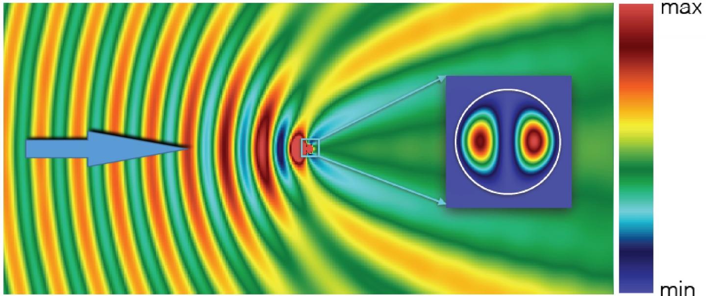
Intensity of the magnetic field at the scattering of an electromagnetic wave. The incident wave propagates from left to right as it is indicated by the blue arrow. The color bar has different scales for the field outside the particle and within it (shown on a larger scale on the insert). CREDIT Michael Tribelsky
Scientists from the Lomonosov Moscow State University together with their Russian and foreign colleagues have done for the first time direct measurements of giant electromagnetic fields, emerging in dielectric particles with the high refractive index at the scattering of electromagnetic waves. The researchers have presented their project results in the Scientific Reports.
The problem of miniaturization of basic elements in electronics requires new approaches. In this connection, it has become very important to be able to create intensive electromagnetic fields concentrated in the smallest possible volume. Scientists from the Lomonosov Moscow State University in collaboration with an international team for the first time conducted direct measurements of a giant resonant field excited inside a subwavelength dielectric particle at the scattering of a plane electromagnetic wave and provided the complete quantitatively theoretical explanation of the observed effect.
Professor Michael Tribelsky, Doctor of Physics and Mathematics and the leading article author, says: “In theory this effect has been known: in this case the scattering particle acts as a funnel, gathering incident radiation from a large area and concentrating it in a small volume within the particle. However, one faces many difficulties on the way of its practical realization. Metallic nanoparticles were the first candidates for such “field concentrators.” Unfortunately, they have deceived the expectations. The point is that metals have high dissipative losses in the most interesting for applications area of visible light frequencies of the incident waves. The dissipation leads to significant energy losses, wasted for fruitless (and often harmful) heating of the nanoparticle, and diminishes the resonant enhancement of the electromagnetic field. In such a case, it would be natural to turn to dielectric particles. Unfortunately, it is not so simple to deal with them too.”
If a particle does not have a high value of its refractive index, the resonant effects are weak. Regarding the high-index particles, whose size is smaller than the wavelength of the incident radiation, the common belief was that the electromagnetic field hardly penetrated in such a particle. However, it has turned out to be that at some frequencies of the incident radiation the case is just the opposite. Namely, the field not only penetrates into the particle, but its giant concentration may be observed. In a sense, the effect is analogous to a gradual swinging of a swing due to weak but made in a proper moment of time pushes.
“Our main result is that, to the best of our knowledge, we are the first who has obtained the direct experimental evidence of the effect and measured the profiles of the excited fields,” — Michael Tribelsky explains.
The difficulties of the corresponding measurements at optical frequencies are related to the fact that one has to measure fields within a nanoparticle, and the spatial resolution of the measurements should be of the order of nanometers! We have overcome the difficulties, modeling the scattering of light by a nanoparticle by means of the identical scattering of radio waves by a centimeter-size particle. To be able to move a probe inside the particle, liquid dielectric (usual distilled water held at a certain fixed temperature) poured into a transparent for the incident radio wave container has been employed.
The research area, to which the project refers to, lies on the very frontier of modern studies on subwavelength optics (namely, optics, dealing with objects whose scales are smaller than the wavelength of the incident radiation). Interest in these phenomena is caused by their extensive applications ranging from medicine (diagnosis and treatment of diseases, including oncological ones; targeted drug delivery and others), biology (various sensors and markers), telecommunications (nanoantennas) to systems for information recording and storage and other spheres. This phenomenon could also be used for the creation of revolutionary new optical computers where information is transferred not by electric pulses but by light packages.
The scientist concludes: “In a broad perspective our project may initiate the creation of a new landscape for design and fabrication of super-miniature nanodevices and metamaterials — namely, materials, which are artificially formed and structured in a special way to possess unusual electromagnetic properties.”


