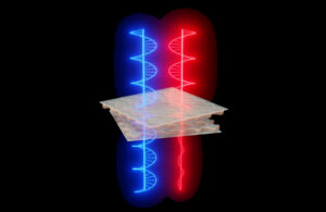
Two stacked photonic crystal slabs transmit right-handed (red) and left-handed (blue) circularly polarized light differently at chiral resonance frequencies. By adjusting the twist angle and spacing between layers, the device can selectively filter one handedness over the other. Credit: Mazur group/Harvard SEAS
Researchers at Harvard SEAS have built a MEMS-integrated photonic crystal device that can actively control the handedness of light passing through it. By stacking two silicon nitride photonic crystal slabs and precisely adjusting their twist angle and spacing with electrostatic actuators, the team achieved measured circular dichroism ranging from −0.85 to 0.64, with simulations showing the architecture can reach the theoretical maximum of ±1. The work, published March 4 in Optica, demonstrates what the researchers describe as a CMOS-compatible platform for dynamic control of intrinsic optical chirality at near-infrared wavelengths — a combination that has proved difficult to achieve in prior nanophotonic designs. The development has implications for chiral molecular sensing, polarization-based optical communications and quantum photonics.
The device draws on principles from twistronics, a field that gained prominence through research on twisted bilayer graphene. Each layer is an individually achiral photonic crystal slab, a nanoscale structure with a periodic square lattice of circular holes. When aligned, the two layers preserve mirror symmetry and show no intrinsic chirality. But when one layer is rotated relative to the other, the mirror symmetries break, and the structure becomes geometrically chiral. That geometric chirality translates directly into different transmission behavior for left- and right-circularly polarized light.
What distinguishes this work from prior approaches is the combination of intrinsic chirality with active tunability. Most previous demonstrations of chirality in nanophotonic structures were either static, locked into a fixed configuration at fabrication, or relied on extrinsic chirality, which depends on the angle of incoming light rather than the structure itself. The Harvard team’s MEMS actuators allow independent control of both the twist angle (tunable from 9° to 13°) and the interlayer gap (from 360 to 1,500 nm), giving them continuous access to a range of chiral responses without swapping components or changing the angle of incidence. The team also identified topologically protected states in the device’s parameter space that can theoretically reach perfect circular dichroism of ±1, a finding that suggests the architecture has room to improve beyond the current experimental results.
The platform’s purely dielectric architecture, which eliminates the ohmic losses that have limited plasmonic approaches, positions it for several applications the authors outline in the paper. In chiral sensing, the device’s tunability could enable compact tools for detecting specific molecular enantiomers at different wavelengths, a persistent challenge in pharmaceutical quality control. In optical communications, the chip could function as a dynamic polarization modulator, controlling light states directly on-chip without swapping out static components. The researchers also point to quantum photonics, where precise polarization control at normal incidence could support spin-selective light sources. Graduate student Fan Du, who led the work in Eric Mazur’s lab, and co-authors write that the all-dielectric device opens pathways for “applications in chiral sensing, dynamic polarization modulation, optical communications, and quantum photonics.”