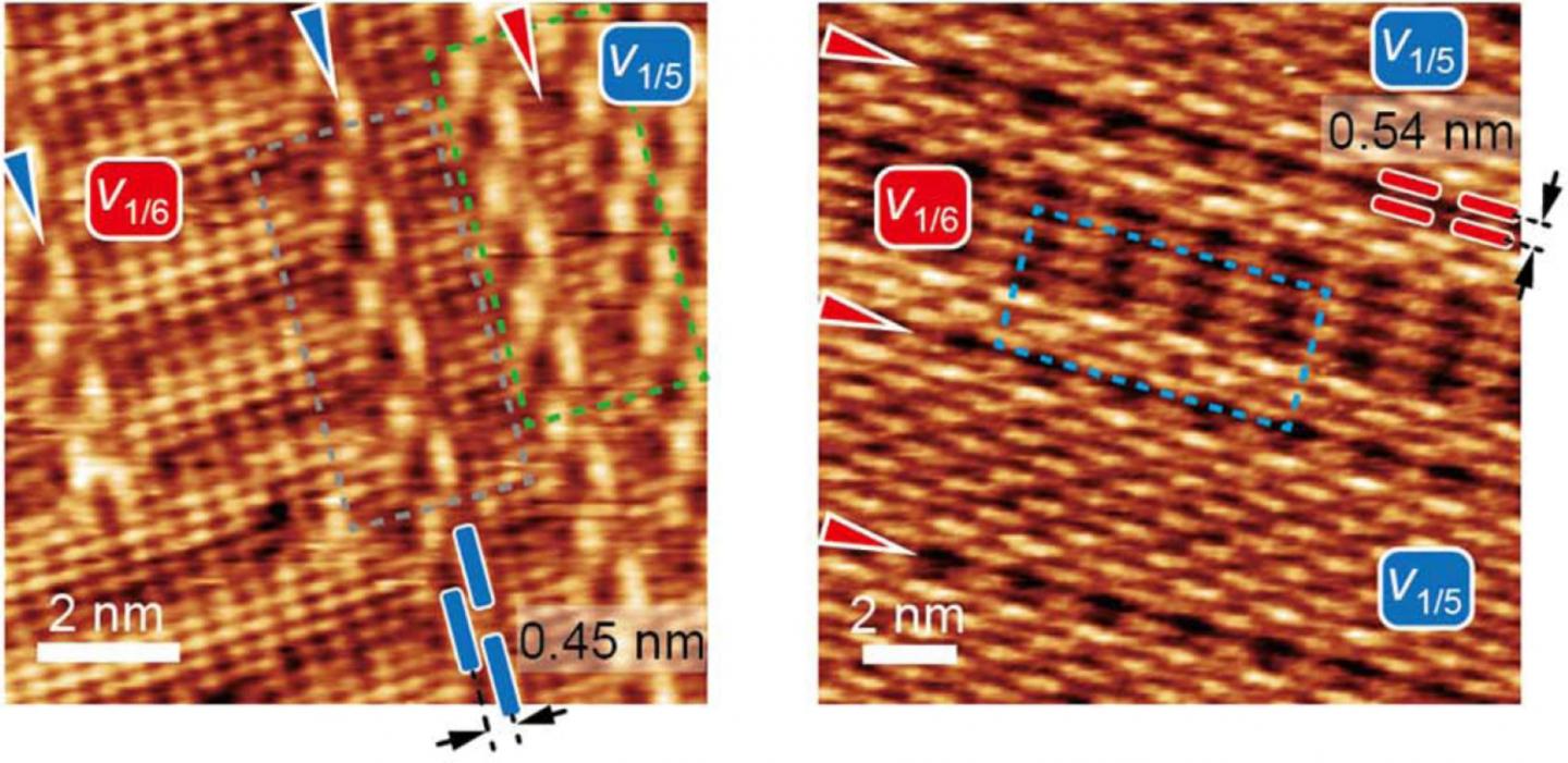
Scanning tunneling electron microscope images of line defects in 1-to-6 and 1-to-5 borophene, indicated by blue and red arrowheads, respectively, show how the defects align in a way that preserves the synthetic material’s metallic nature. Scientists at Rice and Northwestern universities made the first detailed analysis of ordered defect structures in borophene. Credit: Hersam Research Group/Northwestern University
Borophene, the atomically flat form of boron with unique properties, is even more interesting when different forms of the material mix and mingle, according to scientists at Rice and Northwestern universities.
Scientists at the institutions made and analyzed borophene with different lattice arrangements and discovered how amenable the varied structures are to combining into new crystal-like forms. These, they indicated, have properties electronics manufacturers may wish to explore.
The research led by Rice materials theorist Boris Yakobson and Northwestern materials scientist Mark Hersam appears in Nature Materials.
Borophene differs from graphene and other 2D materials in an important way: It doesn’t appear in nature. When graphene was discovered, it was famously yanked from a piece of graphite with Scotch tape. But semiconducting bulk boron doesn’t have layers, so all borophene is synthetic.
Also unlike graphene, in which atoms connect to form chicken wire-like hexagons, borophene forms as linked triangles. Periodically, atoms go missing from the grid and leave hexagonal vacancies. The labs investigated forms of borophene with “hollow hexagon” concentrations of one per every five triangles and one per every six in the lattice.
These are the most common phases the Northwestern lab observed when it created borophene on a silver substrate through atomic boron deposition in an ultrahigh vacuum, according to the researchers, but “perfect” borophene arrays weren’t the target of the study.
The lab found that at temperatures between 440 and 470 degrees Celsius (824-878 degrees Fahrenheit), both 1-to-5 and 1-to-6 phases grew simultaneously on the silver substrate, which acts as a template that guides the deposition of atoms into aligned phases. The labs’ interest was heightened by what happened where these domains met. Unlike what they had observed in graphene, the atoms easily accommodated each other at the boundaries and adopted the structures of their neighbors.
These boundary adjustments gave rise to more exotic – but still metallic – forms of borophene, with ratios such as 4-to-21 and 7-to-36 appearing among the parallel phases.
“In graphene, these boundaries would be disordered structures, but in borophene the line defects, in effect, are a perfect structure for each other,” said Rice graduate student Luqing Wang, who led a theoretical analysis of atom-level energies to explain the observations. “The intermixing between the phases is very different from what we see in other 2D materials.”
“While we did expect some intermixing between the 1-to-5 and 1-to-6 phases, the seamless alignment and ordering into periodic structures was surprising,” Hersam said. “In the two-dimensional limit, boron has proven to be an exceptionally rich and interesting materials system.”
Wang’s density functional theory calculations revealed the metallic nature of the line defects; this implied that unlike insulating defects in otherwise metallic graphene, they have minimal impact on the material’s electronic properties at room temperature. At low temperature, the material shows evidence of a charge density wave, a highly ordered flow of electrons.
Theoretical calculations also suggested subtle differences in stiffness, thermal conductivity and electrochemical properties among borophene phases, which also suggested the material can be tuned for applications.
“The unique polymorphisms of borophene are on full display in this study,” Yakobson said. “This suggests intriguing interplay in the material’s electronic structure through charge density waves, which may lead to tantalizing switchable electronics.”
“As an atomically thin material, borophene has properties that should be a function of the substrate, neighboring materials and surface chemistry,” Hersam said. “We hope to gain further control over its properties through chemical functionalization and/or integration with other materials into heterostructures.”
Yakobson and Hersam also co-authored a recent Nature Nanotechnology perspective about “the lightest 2D metal.” In that piece, the authors suggested borophene may be ideal for flexible and transparent electronic interconnects, electrodes and displays. It could also be suitable for superconducting quantum interference devices and, when stacked, for hydrogen storage and battery applications.