Imagine wafer-thin eyeglasses or a smartphone camera so small it is invisible to the naked eye.
Imagine an aerodynamic sensor that can conform to the exact slope and angle of a jet airplane wing.
Imagine a material that can coat a tank to make it seem to disappear.
These visions of future technologies emerge from a technical paper titled “Inverse-designed broadband all-dielectric electromagnetic metadevices” published online today in Scientific Reports.
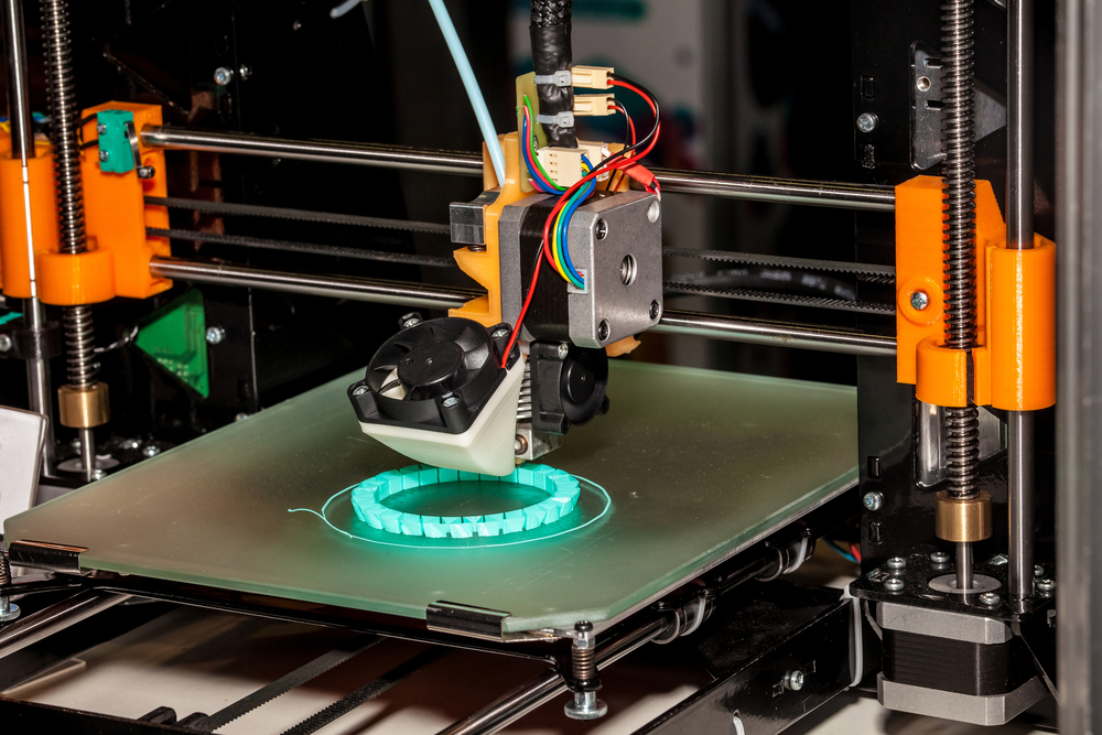
The Northwestern University team used inverse design principles and a basic 3D printer purchased from Amazon — technologies not commonly used in their field– to create highly efficient, non-resonant, broadband metadevices at millimeter-wave frequencies that could prove revolutionary for consumer products, defense, and telecommunications, including next-generation 5G wireless networks.
“I feel like we’re really on the verge of something big,” said Koray Aydin, assistant professor of electrical engineering and computer science at the McCormick School of Engineering, who is leading the research efforts in inverse-designed metadevices. “There’s a lot that needs to be done in the research part, but we’re going in the right direction.”
As opposed to forward design, inverse design starts with a function and asks what structure is needed to achieve the desired result. Using computer modeling, optimization software and complex algorithms, the team set out to build metadevices that could bend or focus millimeter waves but that avoided problems with conventional approaches, such low efficiency, narrow bandwidth and the bulkiness of the devices.
“What we’ve achieved here is a new way of creating electromagnetic devices that achieve certain functions that conventionally seemed impossible to do,” said Prem Kumar, professor of electrical engineering and computer science in McCormick and of physics and astronomy in the Weinberg College of Arts and Sciences. Kumar likened the process to machine learning and said it could produce unexpected outcomes, for example the functionality over a broad bandwidth.
Francois Callewaert, a McCormick School of Engineering graduate student who works with Aydin, developed the inverse design algorithm and performed the numerical simulations. Vesselin Velev, a physics and astronomy graduate student who works with Kumar, helped with the detailed millimeter-wave measurements.
Aydin described the eye-opening moment as the algorithm spit out the design for a complex geometric shape.
“These were not known shapes, not intuitive shapes,” Aydin said.
And that presented its own problem.
“How on Earth are we going to make this?” Aydin recalled thinking. Conventional manufacturing methods would be difficult and expensive. The answer was additive, or 3D, printing.
“This is the heart of the study,” Aydin said. “We’re the first to combine these two to make working devices.”
Kumar agreed. “The important thing to me is the multidisciplinary nature of it,” he said. “We can design a lens in a way that it doesn’t look like a lens.”
Another great strength of their process, Aydin said, was that it was imminently scalable from the microwave to the visible frequency range because of the flexibility of 3D printing.
“It is an exciting result,” said Alan V. Sahakian, the John A. Dever Chair and Professor of Electrical Engineering and Computer Science. “Where in the past somebody might have done a long analysis trying to approximate the behavior, here we essentially input the behavior we wanted into a computer and the computer optimizes a structure that has that behavior and then it comes out the other end of this three-dimensional printer.
“It is truly a breakthrough in the way you can solve problems in a seamless and convenient way.”